Digging deeper: Dielectric Mie voids
Published in Electrical & Electronic Engineering
What lies “Behind a paper”? Ideally, a good story line. In turn, every good story line starts with the right question asked. What is “the right question” might change over time as science seldomly processes in a straight line. Consequently, there is so much more “Behind a paper”.
In our case, the journey started with the paper “Optical Fourier surfaces” by Nolan Lassaline and Co-workers from the David Norris group at ETH Zurich in collaboration with Heidelberg Instruments Nano/SwissLitho (Nature 582, 506 (2020)). In order to arbitrarily shape a reflected optical wavefront, the reflective surface needs to be modulated by a precise sum of sinusoidal waves of appropriate amplitude, spatial frequency, and phase. In order to achieve this demanding goal, the authors employed thermal scanning-probe lithography of appropriate resists which then serve as template for a metallic layer.
Intrigued by the concept, we asked ourselves whether there could be an alternative fabrication strategy. Silicon seemed to be an ideal material as a reusable template, structured by focused ion beam milling (FIB) as an intrinsic grey-scale technique. To our delight, the crystallinity of the substrate resulted in excellent milling results of different structures, perfect as template.
One point, though, seemed to be a nuisance: We continued to observe faint reddish colours, generated by individual voids, with their hue depending on the exact parameters of the voids. While this would not be surprising for periodic structures which can generate diffractive colours, it seemed odd for individual ones and sparked our imagination: Could this be a localized optical mode? Maybe an “inverse Mie resonance”? A similar phenomenon is known in plasmonic systems by virtue of Babinet’s principle, which relates the optical properties of inverse and solid structures. However, this is only valid for perfect electric conductors and thus not for silicon.
We decided to dig deeper, in the truest sense of the word: Increasing the depth of the voids from about one hundred to several hundreds of nanometers resulted in individual voids showing intense colours over the entire visible wavelength range.
Being excited about these results, questions and concerns arose from all directions. From here on it was a true journey down the rabbit hole: Isn’t this just interference or diffraction? Why are these structures so large compared to solid cylindrical silicon resonators? And besides, if this would be true, why do air bubbles in water or glass do not show resonant optical behaviour?
Finally, we needed to combine the expertise of experimentalists and theoreticians to get to the bottom of our findings. We showed that a void in a high index material supports localized resonant modes in close analogy to the well-known Mie modes in high index materials, thus being termed Mie voids, as illustrated in Figure 1a. In fact, the optical properties of both systems - solid and inverse - are described by Mie’s original theory. Intuitively, both systems rely on the same basic working mechanism, namely Fresnel reflection at the interface of higher and lower index materials. Despite the close analogy, there is one paramount difference: Mie voids resonantly confine light in air rather than inside the high-index host material. Due to this confinement in air, the modes do not suffer from loss and dispersion of the dielectric host medium and even allow for resonant confinement of UV light.
These theoretical results allowed us, for example, to answer the above questions: As the resonant behaviour is independent of the period and depends on the diameter and depth (i.e., the volume) the phenomenon is caused neither by diffraction nor by interference. In solid silicon structures the light confinement takes place inside the silicon, thus these structures are about a factor of four (nsilicon ~ 4) smaller compared to Mie voids. The refractive index contrast between air and water (or glass) is too small for resonant confinement. Furthermore, air bubbles have generally a diameter of several micrometers and are thus too large for our phenomenon.
How does one implement such Mie voids experimentally? Instead of creating voids inside a bulk material which is highly absorptive, we bring the voids to the surface and create cylindrical voids in a standard silicon wafer by FIB milling, which is depicted in the SEM images in Figure 1b. Figure 1c displays scanning electron and optical microscope images of individual voids with different depth and diameter. The optical image illustrates the resonant optical behaviour of the voids, showing brilliant colours in reflection.
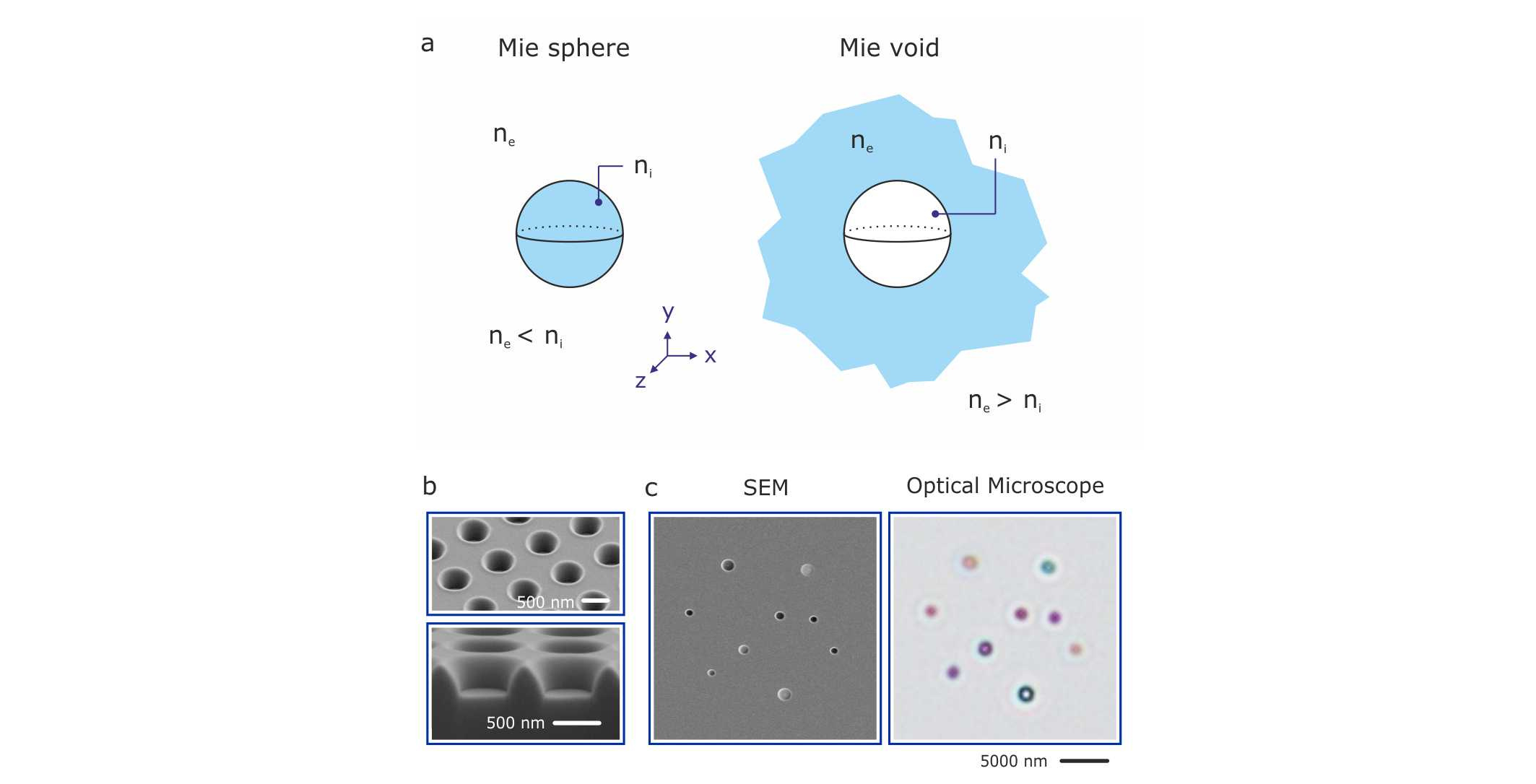
Figure 1: a Concept of Mie voids: Mie theory describes light scattering off spherical inclusions inside a homogenous surrounding. This can refer to a particle of higher refractive index ni a lower refractive index surrounding ne (left), as typically considered for dielectric resonators (ni > ne). In case of a dielectric Mie void (right) the refractive index of the surrounding ne is larger than the refractive index ni of the void material (ni < ne ). In both cases localized optical modes emerge, which are confined within the volume of the spherical inclusions – in case of the Mie void light can consequently be trapped inside a low-loss medium. b Experimental implementation of Mie voids as cylindrical voids in a silicon surface (normal view and FIB cut). c Scanning electron and optical microscope image of Mie voids illustrate the visible colour appearance.
The most intriguing property of Mie voids is the resonant confinement in air, allowing to confine radiation even in wavelength regions in which the host material strongly absorbs. Even more surprising, and highly counterintuitive at first sight: Loss in the host material increases the confinement strength as the Fresnel reflection increases with increasing refractive index and loss. We could experimentally demonstrate resonant confinement of UV radiation down to 265 nm (at a photon energy of 4.68 eV).
While these results have the most profound implications, the colour generated by the voids is the most fascinating aspect for most people. Indeed, the optical response of the individual voids (which can be tuned over the entire visible wavelength range) combined with the off-resonant reflection of the bare silicon substrates results in spectral features of ideal linewidth for brilliant, intense, and naturalistic colours. Mie voids are therefore ideal candidates for nanoscale colour-printing at highest resolution.

Figure 2: Mie void-based nanoscale colour-printing at 36.000 dpi resolution: Section of “Improvisation No. 9" by Wassily Kandinsky. Left: Original image and reproduced colour-print. Right: SEM image of the colour-print.
As an example, we choose the painting “Improvisation No. 9” (Wassily Kandinsky, Staatsgalerie Stuttgart, Germany). Figure 2 depicts a section of the original painting and its experimentally colour-printed version. The period is kept constant at 900 nm, ruling out any grating effect. Each pixel is thus composed of one Mie void each. As a consequence, even in the SEM image (shown on the right) the contours and different components of the painting can be clearly identified. Additionally, it is obvious that the diameter and depth of the Mie voids serve as colour tuning knobs. Comparing the original painting and its colour-printed counterpart, we find that the colour reproduction is excellent, which is aided by the availability of “white” and “black” hues, that enable us to achieve large dynamic range and good contrast.
Mie voids offer unique properties that will aid many fields of nanophotonics. They will push the operation of functional high-index metasurfaces into the blue and UV spectral range. The combination of resonant dielectric Mie voids with dielectric nanoparticles will more than double the parameter space for the future design of metasurfaces and other micro- and nanoscale optical elements. In particular, this extension will enable novel antenna and structure designs which benefit from the full access to the modal field inside the void as well as the nearly free choice of the high-index material for novel sensing and active manipulation strategies.
Follow the Topic
-
Light: Science & Applications
A peer-reviewed open access journal publishing highest-quality articles across the full spectrum of optics research. LSA promotes frontier research in all areas of optics and photonics, including basic, applied, scientific and engineering results.







Please sign in or register for FREE
If you are a registered user on Research Communities by Springer Nature, please sign in