Downscaling two-dimensional integrated circuits by using ultrathin high-κ magnesium niobate single crystals
Published in Physics

Two-dimensional (2D) van der Waals (vdW) semiconductors are considered as ideal building blocks of post-Moore field effect transistors (FETs) and integrated circuits for sub-5 nm technology nodes. The full delivery of theoretical performance of FETs requires compatible 2D high-dielectric-constant (κ) materials with excellent electric insulativity. It not only guarantees the low leakage current and efficient gate controllability, but also allows the flexible vdW integration of an ideal dielectric/semiconductor heterointerface with eliminated defects and interface charge traps for superior electron transport. However, implementation of devices with low power consumption and high reliability remains challenging, since the existing 2D insulators usually cannot provide the best trade-off for requirement in terms of wide band gap, large breakdown strength, high dielectric constant, small leakage current, and great bias temperature stability.
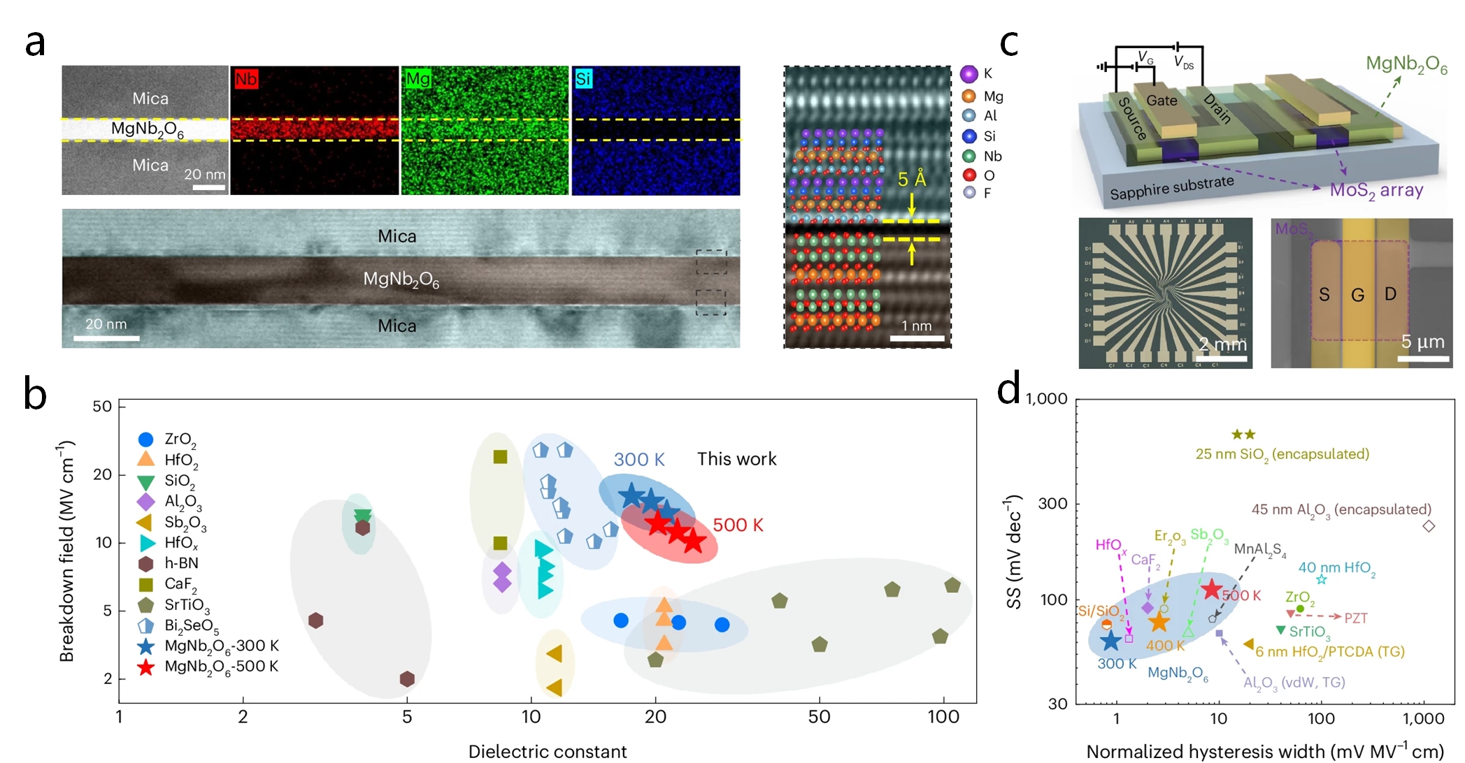
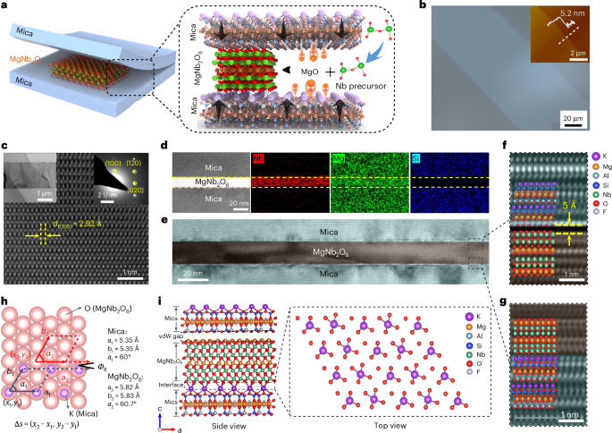
Magnesium niobate (MgNb2O6) is a dielectric ceramic that is used extensively for microwave filters and resonators. With the assistance of a buffer-controlled epitaxy growth process on a mica substrate, the thickness downscaling of single-crystalline MgNb2O6 were initially realized (Figure 1a). Compared with the reported dielectric materials applied in the state-of-art Si and 2D semiconductor technologies, the ultrathin MgNb2O6 crystals demonstrate a well-balanced breakdown strength and dielectric constant over a wide temperature range (Figure 1b). In addition, ultrathin MgNb2O6 crystals reveal excellent thermal stability and electrical reliability, which are of significant importance for device applications. It still retains a large EBD up to 10 MV cm−1 even at a high testing temperature of 500 K, together with a small leakage current in order of 10−2 A cm−2 under 5 MV cm−1. With an operation field strength of 2.5 MV cm−1, the lifetime towards device failure is predicted to be as long as 100 years.
The excellent dielectric properties, together with great thermal stability and electrical reliability, enable crystalline MgNb2O6 an ideal insulating candidate to be integrated into 2D semiconducting channels for high-performance FETs, highlighting its great potential for future 2D nanoelectronics. Monolayer molybdenum disulfide (MoS2) FETs integrated with MgNb2O6 gate dielectric exhibit a hysteresis of 0.9 mV/(MV cm−1), steep subthreshold swings of 62 mV dec−1, on/off current ratio up to 4 × 10⁷, and operation reliability at temperatures up to 500 K, which can meet the requirements of the 2022 International Roadmap for Devices and Systems (IRDS) for low-power transistors (Figure 1c-d). The excellent electrostatic controllability of MgNb2O6 also allows us to fabricate graphene-contacted short-channel FETs and inverter circuits with a length limit of only 50 nm.

Fig. 1 | Magnesium niobate as a high-κ gate dielectric for two-dimensional electronics a, High-resolution transmission electron microscope (HRTEM) image images of the heterojunction area between MgNb2O6 nanosheet and mica substrate, where sharp and clean interfaces can be identified. b, Breakdown field (EBD) versus effective dielectric constant (εr) of ultrathin MgNb2O6, compared with various dielectric materials. c, Schematic and OM image of the top-gated monolayer MoS2 FETs array consisting of 20 individual devices. The width and length of the channel are patterned to be 10 and 4  m, respectively. d. The SS values coupled with normalized hysteresis of MgNb2O6-gated monolayer MoS2 FETs compared with literatures.
Our work demonstrated an important step for achieving high-performance FETs with atomic size and ultra-short channel beyond Moore’s law. The development of ultrathin crystalline MgNb2O6 can help in the design and fabrication of future electronic devices via vdW integration strategy, offering a potential route to implement 2D FETs on very-large-scale integration chips.
Jing-Kai Qin
Dr. Qin is currently an associate professor in School of Integrated Circuits, Harbin Institute of Technology Shenzhen, China. He is a researcher in the field of nano electronics, and his main research focuses on low-dimensional nanomaterials and their applications for electronics, optoelectronics and neuromorphic devices.
Follow the Topic
-
Nature Electronics
This journal publishes both fundamental and applied research across all areas of electronics, from the study of novel phenomena and devices, to the design, construction and wider application of electronic circuits.


Please sign in or register for FREE
If you are a registered user on Research Communities by Springer Nature, please sign in