Evanescent-field-induced rapid loss of high-k information may cause the near-field OPE
Published in Electrical & Electronic Engineering

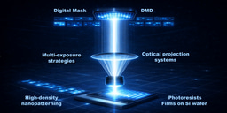
With the rapid increase in the integrated degree and the feature size of integrated circuits continue to decrease in pace with the Moore’s law, the imaging quality of near-field lithography has been badly affected by the optical proximity effect (OPE), particularly when the critical dimension (CD) reaches to the achievable resolution of near-field lithography [1]. To reduce the effect of OPE on image quality and enhance the resolution and image contrast of the generated aerial image of near-field lithography, many kinds of resolution enhancement techniques (RETs) have been proposed, such as off-axis illumination (OAI), phase-shifting masks (PSMs), optical proximity correction (OPC) [2-5]. However, a detailed understanding of the OPE in near-field, for an accurate nanometer scale patterning with quantitative proximity correction and compensate image distortion still constitutes an open challenge.
The aim of our study was therefore to investigate the physical origin of the near-field OPE in an evanescent-field-based patterning system, and then proposed a new OPC method based on the spatial modulation of evanescent waves in near-field, with the goal of improving the ultimate achievable pattern fidelity.
Plasmonic lithography is one kind of the near-field lithography. For a maskless plasmonic lithography with a bowtie-shaped nanoaperture (BNA), the BNA serves as a local near-field optical source and at the exit of the BNA, surface plasmon waves are exploited to generate high spatial-frequency (k) evanescent fields in the photoresist layer [6]. Numerical calculations have been carried out to evaluate the achievable fidelity of the plasmonic lithography and quantitatively analyze the near-field enhancement effect and the size-dependence of plasmonic near-field, with aim to estimate the point-spread function with accuracy and efficiency. Furthermore, an analytical formula was proposed to quantitative analysis the effect of the rapidly decaying feature of evanescent field on the near-field OPE, and the theoretical limit of the pattern fidelity.
Our theoretical calculations and simulation results indicate that the evanescent-field-induced rapid loss of high-k information is one of the main optical contributors to the near-field OPE. Notably, a fast and effective OPC method based on the compensation principle of exposure dose was proposed to relax the pattern distortion by spatially modulating the exposure map with dose leveling. Using the near-field OPC-assisted patterning strategy, the final pattern fidelity can be greatly enhanced.
References
- Liebmann,, Mansfield, S., Wong, A., Lavin, M., Leipold, W., & Dunham, T. TCAD development for lithography resolution enhancement. IBM J. Res. Dev. 45, 651–665 (2001).
- Yao,N., Lai, Z., Fang, L., Wang, C., Feng, Q., Zhao, Z., & Luo, X. Improving resolution of superlens lithography by phase-shifting mask. Express 19, 15982-15989 (2011).
- Huang, Q.,Wang, C., Yao, N., Zhao, Z., Wang, Y., Gao, P., Luo, Y., Zhang, W., Wang, H., & Luo, X. Improving imaging contrast of non-contacted plasmonic lens by off-axis illumination with high numerical aperture. Plasmonics 9, 699-706 (2014).
- Luo,Y., Liu, L., Zhang, W., Kong, W., Zhao, C., Gao, P., Zhao, Z., Pu, M., Wang, C., & Luo, X. Proximity correction and resolution enhancement of plasmonic lens lithography far beyond the near field diffraction limit. RSC Adv. 7, 12366-12373 (2017).
- Oh,S., Han, D., Shim, H. B., & Hahn, J. W. Optical proximity correction (OPC) in near-field lithography with pixel-based field sectioning time modulation. Nanotechnology 29, 045301 (2018).
- Kim,, Jung, H., Kim, Y., Jang, J., & Hahn, J. W. Resolution limit in plasmonic lithography for practical applications beyond 2x-nm half pitch. Adv. Mater. 24, OP337–OP344 (2012).
Follow the Topic
-
Microsystems & Nanoengineering

This journal, with a target for a high-end journal for years to come, seeks to promote research on all aspects of microsystems and nanoengineering from fundamental to applied research.


Please sign in or register for FREE
If you are a registered user on Research Communities by Springer Nature, please sign in