Exploring GeS₂ to Rethink Photonic Devices
Why We Need Better Materials to Shape Light
In the race to miniaturize technology, photonics stands out: it’s about controlling light the way electronics control electrons. For applications like AR/VR headsets, smart contact lenses, LiDAR systems, and integrated biosensors, the core challenge is finding materials that can bend and guide light efficiently without adding bulk. High refractive index (high-n) materials are essential here, enabling thinner and lighter waveguides, increasing the field of view in wearables, and boosting performance in compact optical systems.
Traditionally, photonic systems rely on high-n materials like silicon, titanium dioxide (TiO₂), or gallium phosphide (GaP). These offer good light confinement but come with trade-offs – silicon, for instance, is opaque in the visible range.
This limitation has driven interest in alternative material platforms. Van der Waals (vdW) materials are layered compounds whose atomic sheets are bonded weakly by intermolecular forces. They have emerged as potential game-changers in nanophotonics, thanks to their extraordinary optical properties. Yet a major limitation remained: no known vdW material combined a high refractive index with transparency across the full visible spectrum. This is crucial for optical devices because they need to let all colors of light pass through clearly. If any part of the visible spectrum is lost or distorted, images can become blurry or inaccurate. This transparency gap stalled progress.
We set out to address this bottleneck by investigating germanium disulfide (GeS₂), a material with a wide bandgap and promising optical traits, aiming to add a much-needed option to the vdW material family for visible-light technologies.
What Makes GeS₂ Stand Out
GeS₂ brings together three rare and valuable optical traits.
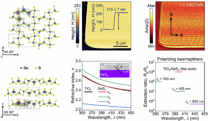
It has a high refractive index of around 2.6 and stays transparent across the entire visible range – two features we’ve already touched on above.
What really sets it apart, though, is its strong optical anisotropy—GeS₂ interacts with light differently depending on its direction of travel. This directional dependence, known as birefringence, is remarkably large: up to 0.12 between in-plane axes and 0.63 out-of-plane. That gives engineers much more flexibility to tune how light behaves in a device by adjusting the crystal’s orientation or the light’s polarization.
Other materials can offer high index or transparency, but rarely both – let alone with this level of anisotropy.
In contrast to isotropic materials like TiO₂, which behave the same in all directions, GeS₂ offers multiple optical responses in one material – turning it into a versatile building block for next-generation photonics.
A Real-World Example: The Polarizing Beamsplitter
To illustrate GeS₂’s real-world potential, we modeled a polarizing beamsplitter based on a GeS₂/TiO₂ interface. When s-polarized light (aligned with GeS₂’s a-axis) hits the interface, it sees little difference in refractive index and passes through. But p-polarized light (sensitive to GeS₂’s b- and c-axes) reflects strongly.
This results in a highly efficient polarization filter, with extinction ratios up to 10⁶– better than current commercial devices. Pairing GeS₂ with industry-standard TiO₂ demonstrates how it can enhance, not replace, existing photonic technologies.
Why We’re Exploring GeS₂ and Where It Could Go Next
This research wasn’t driven by curiosity alone. The kinds of materials we studied here –thin, transparent, and optically powerful – are exactly what’s needed for applications like smart contact lenses and other wearable photonic devices. At XPANCEO, where we’re working to bring such technologies to life, studies like this are a key part of the process.
While GeS₂ shows exciting optical performance, the next big step is figuring out how to produce it at scale. Current lab methods like manual exfoliation are great for exploring properties, but not yet suited for large-area device manufacturing.
Developing scalable growth techniques such as epitaxy is a natural next move. It’s already making progress with other vdW materials and could work for GeS₂ too.
Once that becomes possible, we’ll likely see GeS₂ powering slimmer AR glasses, denser optical circuits, smarter ways to control light – and perhaps even components inside a contact lens. It's doing great in the lab – and with a little help, it might just escape it.
Follow the Topic
-
Light: Science & Applications
A peer-reviewed open access journal publishing highest-quality articles across the full spectrum of optics research. LSA promotes frontier research in all areas of optics and photonics, including basic, applied, scientific and engineering results.


Please sign in or register for FREE
If you are a registered user on Research Communities by Springer Nature, please sign in