Physics of 2D Materials for Developing Smart Devices

As the demand for smarter, smaller, and more energy-efficient electronics surges, the limits of conventional 3D semiconductors are becoming impossible to ignore. Now, researchers from Netaji Subhas University of Technology and the Institute of Infrastructure Technology Research & Management—led by Dr. Neeraj Goel and Dr. Rahul Kumar—have published a comprehensive review on the fundamental physics of two-dimensional (2D) materials and their roadmap toward smart-device deployment. The work distills two decades of progress into a single, forward-looking guide for physicists, materials scientists, and circuit engineers.
Why 2D Physics Matters
• Quantum Confinement: When crystals are thinned to a single unit cell, their electronic band structure, phonon spectrum, and dielectric response change dramatically, enabling properties unattainable in bulk.
• Statistical Transport: Atomically thin membranes exhibit ballistic transport, unconventional heat capacity, and gate-tunable carrier densities that translate directly into ultra-low-power switches and sensors.
• Van-der-Waals Engineering: Because 2D layers are bonded in-plane by covalent forces and out-of-plane only by weak vdW interactions, they can be stacked into defect-free heterostructures without lattice-matching constraints, opening an entirely new device design space.
Innovative Design Levers
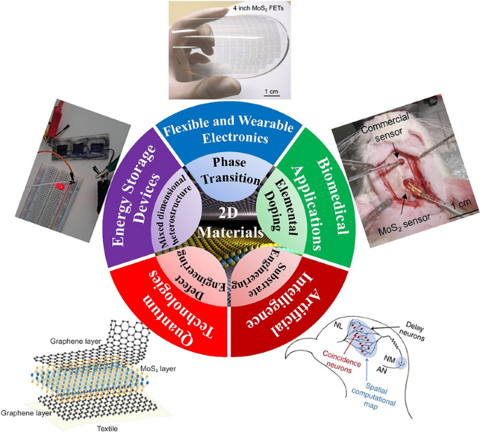
• Material Palette: The review catalogs graphene (zero-gap semimetal), transition-metal dichalcogenides (TMDs, 1–2 eV direct gap), hexagonal boron nitride (wide-gap insulator), phosphorene (tunable 0.3–2 eV gap), and emerging MXenes, enabling metallic, semiconducting, magnetic, superconducting, and ferroelectric building blocks in one compatible platform.
• Phase & Defect Engineering: 2H-to-1T phase transitions, controlled doping, strain-induced bandgap renormalization, and intentional vacancy creation are highlighted as non-destructive knobs to tailor carrier type, density, and spin polarization.
• Mixed-Dimensional Heterostructures: 2D/3D (e.g., MoS2/Si) and 2D/2D (e.g., graphene/h-BN) stacks are shown to decouple the conflicting requirements of high mobility, high on/off ratio, and CMOS-back-end-of-line thermal budget.
Applications & Future Outlook
• Sub-1 nm FETs: Monolayer MoS2 channels with carbon-nanotube gates have already delivered 1 nm gate-length transistors with 106 on/off ratio, proving that 2D materials can extend Moore’s law when silicon cannot.
• Flexible & Wearable ICs: Wafer-scale CVD MoS2 on PET substrates yields inverters with voltage gain ≈ 400 and power < 10 pW µm-1 at 1 V, enabling roll-to-roll circuits for e-skin and smart textiles.
• Neuromorphic Synapses: Gate-tunable hysteresis in polycrystalline MoS2 memtransistors emulates long-term potentiation/depression with sub-fJ energy per spike, providing a hardware path for energy-frugal AI.
• Quantum Technologies: Strong spin–orbit coupling in TMDs and atomically sharp h-BN defects are leveraged for room-temperature single-photon emitters and spin-qubit hosts, positioning 2D materials as front-runners for on-chip quantum communication and sensing.
• Energy & Sensing: Graphene/MoS2 hybrid supercapacitors achieve > 100 mF cm-2 areal capacitance, while defect-engineered MoS2 films act as room-temperature NO2 sensors with single-ppb resolution, demonstrating simultaneous advances in storage and environmental monitoring.
Challenges & Opportunities
The review closes by identifying critical roadblocks—air stability of phosphorene, scalable growth of single-crystal TMDs on 300 mm Si, and reliable low-resistance contacts for sub-5 nm nodes—and outlines interdisciplinary strategies spanning surface chemistry, heterogeneous integration, and in-situ metrology to overcome them.
This comprehensive roadmap provides a physics-based blueprint for transforming atomically thin crystals into mainstream smart devices. Stay tuned for more breakthroughs from Dr. Neeraj Goel and Dr. Rahul Kumar as they push 2D materials from lab curiosity to foundry reality!
Editor of Nano-Micro Letters, which is an Open-Access, peer-reviewed journal reported papers that have at least one dimension ranging from a few sub-nanometers to a few hundreds of micrometers. The journal is published by Springer Nature and indexed by SCI, EI, SCOPUS, Pubmed, etc. The 2025 JCR Impact Factor is 38.5. The 2025 CiteScore is 58.9.
Follow the Topic
-
Nano-Micro Letters
Nano-Micro Letters is a peer-reviewed, international, interdisciplinary and open-access journal that focus on science, experiments, engineering, technologies and applications of nano- or microscale structure and system in physics, chemistry, biology, material science, and pharmacy.


Please sign in or register for FREE
If you are a registered user on Research Communities by Springer Nature, please sign in
Very Interesting article