Residue-free wafer-scale direct imprinting of two-dimensional materials
Background and Challenge
Monolayer two-dimensional (2D) materials, with their angstrom-scale thickness (about one millionth of a human hair), represent the bleeding edge of semiconductor innovation. Materials like molybdenum disulfide (MoS₂) exhibit extraordinary electrical conductivity, optical transparency, and quantum phenomena unmatched by conventional silicon. For decades, scientists have seen them as potential saviors of Moore’s Law—the principle predicting the relentless miniaturization of computing power. Yet, harnessing these atomically thin crystals has proven maddeningly difficult. Traditional micro-fabrication tools, designed for manipulating three-dimensional "bulk" materials, are fundamentally mismatched for handling near-weightless, single-atom-thick films. The slightest contamination—even a stray polymer residue or chemicals—can disrupt their pristine atomic surfaces, degrading their performance and undermining scalability. Achieving large-area, high-yield production of uncontaminated 2D films became the field’s "holy grail"—and its most persistent bottleneck.
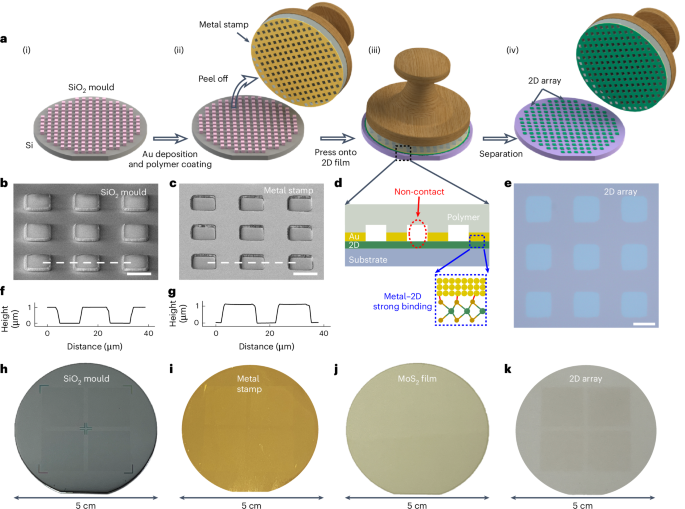
During my PhD research (2020–2021), I pioneered an approach using metal-mesh to dry-transfer large-area MoS₂ films directly from bulk crystals—avoiding the wet chemicals that typically leave residues. This "metal-mesh assisted exfoliation" showed promise, producing arrays of monolayer material. But a critical flaw remained: the 2D flakes still contacted polymer supports during transfer, compromising surface purity. Atomic perfection remained out of reach. I envisioned a radical redesign: a fully suspended, three-dimensional micro-grid. The goal was to achieve a local contact mode, its recessed geometry would only touch the 2D material at isolated region, leaving the rest untouched and intrinsically clean. To obtain this structure, my first idea was to create a pattern template on the silicon substrate using the commonly used photoresist in the laboratory and then create a three-dimensional structural grid with local depressions.
Failure followed failure. Photoresists proved too soft, thermally unstable, and prone to peeling. Neither "positive" nor "negative" variants could maintain structural integrity at microscale dimensions. My lab notebooks filled with images of collapsed grids and deformed templates. After years of struggle, the project stalled—a promising idea trapped by material limitations.
Inspiration from historic movable type printing
In late 2023, a breakthrough arrived unexpectedly. On a sunlit morning at Nanyang Technological University (NTU), Singapore, while watching a video about historic Chinese movable-type printing over breakfast, I connected its template structure to my "local-contact" concept. I realized the template material need not be limited to photoresists—any durable substance could work.

Within 24 hours, I adapted a microfabrication process to upgrade the mold and stamp:
- Lithographically define a photoresist pattern.
- Deposit silicon dioxide (SiO₂) onto Si substrate and lift off to fabricate the mold.
- Evaporate 50-nm-thick gold metal onto the SiO₂/ Si mold as the functional layer.
- Spin coating a polymer supporting layer to peel off the 3D metal and prepare an Au-stamp.
Holding this "3D stamp," I pressed it gently onto a sheet of 2D chemical-vapor-deposited (CVD) MoS₂. Like paper adhering to template, the 2D crystal only attached to the stamp’s raised contours. When I lifted the stamp, what remained was a flawless, contamination-free MoS₂ pattern—atomic smoothness preserved everywhere the stamp hadn’t touched. Thrilled by the result, I immediately shared it with my advisor, Prof. Weibo Gao. We jointly mapped out detailed optical/electrical characterization plans, confident in this novel technique.
a, Method steps: (i) depositing SiO2 mold array on silicon wafer; (ii) depositing gold film on the SiO2 mold and spin-coating the surface with polymer to fabricate a 3D metal-stamp, and peeling off; (iii) pressing 3D metal stamp onto a 2D wafer; (iv) separating the metal stamp from 2D film and obtaining 2D arrays. b, c, SEM images of SiO2 mold and metal-stamp. The metal-stamp inherits the inverted 3D morphology of the silicon mold. Scale bar, 10 μm. d, The cross-section schematic of 3D metal-stamp pressed onto 2D film with local contact model. The metal-2D contact region forms a strong interaction, while the 2D material in the non-contact area retains the original state. e, Optical image of patterned monolayer MoS2 arrays on sapphire substrate. f, g, AFM measurements of 3D morphology of SiO2 mold and metal stamp.
Team and Cooperation
Over the next year, our team meticulously validated the "imprint transfer" technique. We fabricated hundreds of transistors on millimeter-sized CVD films. Compared to devices made via plasma etching—the industry standard—our stamped arrays showed:
- Zero polymer residues on 2D materials surfaces
- 20 times lower variation of threshold voltage
- High uniformity across 100 devices
This rapid progress owed much to our team—supported by many Doctors and Professors including Prof. Hongbing Cai (University of Science and Technology of China), Prof. Zheng Liu (NTU), and Prof. X. Renshaw Wang (NTU)—executed hundreds of devices tests on millimeter-to-centimeter-scale CVD materials. Large-area devices fabricated via stamping outperformed traditional etching methods in both performance and uniformity. To validate industrial scalability, we contacted and collaborated with Prof. Taotao Li (Nanjing University, China), acquiring wafer-scale high-quality monolayer MoS2 films. Using our stamping technique, we patterned these into wafer-scale arrays and fabricated 500 transistors and logic gates, achieving a remarkable 97.6% yield—proving its high-throughput potential. Finally, atomistic modeling by Prof. Ju Li (Massachusetts Institute of Technology, USA) reinforced the method’s theoretical foundation.
Why This Method Matters
This "stamp imprinting" technique isn’t just a lab curiosity—it bridges ancient craftsmanship spanning nearly 1,000 years with the new materials manufacturing at atomic scale. By eliminating contamination at the source, it preserves the advantages of 2D materials while enabling industry-standard wafer processing. With 97.6% yields already achieved, it offers a realistic path toward commercial devices: high-performance transistors, large-scale logic gates, integrated circuits, and perhaps even successors to silicon chips.
Follow the Topic
-
Nature Electronics
This journal publishes both fundamental and applied research across all areas of electronics, from the study of novel phenomena and devices, to the design, construction and wider application of electronic circuits.


Please sign in or register for FREE
If you are a registered user on Research Communities by Springer Nature, please sign in