Supercurrent Modulation in Josephson Junctions by Scanning Gate Microscopy
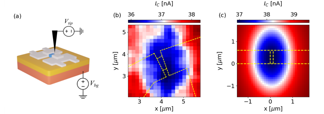
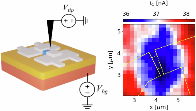
 Graphical representation of a Scanning Gate Microscopy experiment. The light blue section corresponds to the exposed semiconducting region of the junction. (b) SGM map measurement: 20 pixel × 20 pixel critical current map as a function of the position of the tip. Tip voltage Vtip = −10V, back gate voltage Vbg = 9.5V. Yellow dashed lines correspond to the outline of the device. (c) Numerical simulation of a tip-induced critical current modulation map.")
Fig: (a) Graphical representation of a Scanning Gate Microscopy experiment. The light blue section corresponds to the exposed semiconducting region of the junction. (b) SGM map measurement: 20 pixel × 20 pixel critical current map as a function of the position of the tip. Tip voltage Vtip = −10V, back gate voltage Vbg = 9.5V. Yellow dashed lines correspond to the outline of the device. (c) Numerical simulation of a tip-induced critical current modulation map.
Electricity is at the basis of modern technology: most of the objects surrounding us work thanks to streams of electrons flowing through them. But what do these streams look like? Can we visualize them in any way? Given the quantum nature of electrons, do they display interference effects?
With these questions in mind, Scanning Gate Microscopy was developed by Westervelt’s group in Harvard in the 1990s. Its basic principles are the following:
- To obtain quantum interference effects in the electron flow, such flow must be coherent; to ensure that, we want to visualize electron flow in nano-scaled objects at cryogenic temperatures.
- It must be possible to perturb the electron flow to visualize it; if the device under study is made from a semiconductor, we can achieve this by applying external voltages through control electrodes (the same principle is at the basis of field effect transistors).
- To be able to resolve the patterns of electron flow, it must be possible to perturb the electron flow locally. This can be achieved by using an atomically sharp Atomic Force Microscopy tip as a movable gate electrode. The tip can create a barrier that selectively blocks the flow of electrons in its proximity; by recording the conductance of the sample as a function of the position of the tip it is possible to reconstruct the features of the electron flow in the device under study.
In the last three decades, this technique has been applied to successfully visualize and manipulate electron flow in a variety of materials, devices, and by multiple groups across the globe. But why limiting ourselves just to electrons?
Superconductivity has been a hot topic since its discovery; in superconductors current is carried by a collective coherent flow of pairs of electrons: Cooper pairs. When a natural superconductor is galvanically connected to a region of a non-superconducting normal material, i.e. a semiconductor, Cooper pairs can extend into the normal material: this gives rise to the well-known superconducting proximity effect. Thanks to this phenomenon, if a Superconductor-Semiconductor-Superconductor junction is clean enough, Cooper pairs can flow between the superconducting electrodes across the semiconductor region, generating a supercurrent.
What’s more, the semiconductor region of the junction can still be controlled electrostatically! This implies that by studying this kind of devices with a Scanning Gate Microscope we can use the tip to generate a local, movable barrier that selectively blocks the flow of Cooper pairs in its proximity. If, instead of recording the resistance of the junction as a function of the position of the tip (due to superconductivity, it would always be zero), we record its critical current (that is the maximum dissipation-less current the junction can sustain), we could reconstruct the features of the superconducting flow across it. Specifically, this could give insight into the distribution of defects in the junction or allow to visualize magnetic field-induced features like Josephson vortices.
Why has nobody done this so far? Well, because applying Scanning Gate Microscopy to superconducting samples is not easy at all!
- The tip can act as a huge antenna (compared to the size of the device): high frequency noise can completely suppress superconductivity in Josephson junctions if the system is not filtered sufficiently.
- Placing a charged metallic tip close to an exposed semiconductor can cause discharges that can compromise the integrity of the device.
- The experiment must be performed at sufficiently low temperature to ensure the presence of superconductivity (300 mK for our InSb nanoflag-based devices): combining cryogenic equipment with the vibration-free environment required to avoid tip-sample collisions is a challenge.
In 2025, we finally demonstrated the possibility of manipulating the supercurrent flow in junctions using Scanning Gate Microscopy. Our measurements are in excellent agreement with numerical simulations. This is just the first step in the development of the technique: we look forward to improving the resolution to be able to investigate local features in the supercurrent flow.
Have a look at our study here: https://doi.org/10.1038/s43246-025-01000-0
Follow the Topic
-
Communications Materials
A selective open access journal from Nature Portfolio publishing high-quality research, reviews and commentary in all areas of materials science.
Related Collections
With Collections, you can get published faster and increase your visibility.
Smart windows for sustainable buildings
Publishing Model: Open Access
Deadline: Oct 31, 2026
Lead-free perovskite solar cells
Publishing Model: Open Access
Deadline: Oct 31, 2026

Please sign in or register for FREE
If you are a registered user on Research Communities by Springer Nature, please sign in