Two-Dimensional Materials, the Ultimate Solution for Future Electronics and Very-Large-Scale Integrated Circuits
Published in Electrical & Electronic Engineering, Materials, and Physics

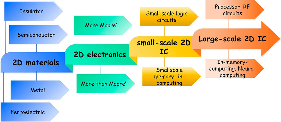
A groundbreaking review published in Nano-Micro Letters provides a comprehensive overview of the role of two-dimensional (2D) materials in shaping the future of electronics and integrated circuits (ICs). Authored by Laixiang Qin and Li Wang from the Ningbo Institute of Digital Twin and Eastern Institute of Technology, the review highlights the potential of 2D materials to overcome the limitations of traditional semiconductors like silicon (Si) and sustain Moore's Law in the post-Moore era.
Why This Research Matters
- Overcoming Silicon Limitations: As the semiconductor industry approaches sub-10 nm technology nodes, traditional bulk semiconductors like Si face significant challenges, including degraded carrier mobility and increased power consumption. 2D materials, with their unique electronic properties, atomic thickness, and ability to maintain high carrier mobility even at sub-1 nm thickness, emerge as superior candidates to address these issues.
- Enabling More-than-Moore Applications: Beyond traditional computing, modern life demands diverse applications such as 5G/6G communication, artificial intelligence, and neuromorphic computing. 2D materials offer the potential for multifunctional integration, enabling the development of flexible electronics, sensors, and in-memory computing devices that meet these advanced requirements.
Innovative Design and Mechanisms
- 2D Materials for Electronics: The review comprehensively covers various 2D materials, including transition metal dichalcogenides (TMDCs), black phosphorus (BP), hexagonal boron nitride (h-BN), and graphene. These materials exhibit a wide range of electronic properties, from insulators to semiconductors and metals, making them suitable for diverse applications.
- Advanced Device Structures: The study explores advanced device structures such as tunnel field-effect transistors (TFETs), negative capacitance field-effect transistors (NCFETs), and impact-ionization FETs (I-IFETs) based on 2D materials. These devices offer steep subthreshold slopes and high on/off ratios, significantly reducing power consumption and improving performance compared to traditional silicon-based devices.
- 3D Integration and Flexible Electronics: The review highlights the potential of 2D materials for 3D monolithic integration, enabling the fabrication of high-density, low-power integrated circuits. Additionally, the mechanical flexibility and robustness of 2D materials make them ideal for flexible and wearable electronics, opening up new possibilities for applications in healthcare, IoT, and consumer electronics.
Applications and Future Outlook
- In-Memory Computing and Neuromorphic Devices: 2D materials-based memristors and memtransistors offer significant potential for in-memory computing and neuromorphic applications. These devices can perform logic operations and data storage simultaneously, reducing latency and power consumption compared to traditional von Neumann architectures.
- High-Performance Logic and Memory Circuits: The review showcases various small-scale and large-scale integrated circuits based on 2D materials, including inverters, logic gates, and memory arrays. These circuits demonstrate promising performance, with high gain, low power consumption, and excellent stability, paving the way for future high-performance computing applications.
- Future Research Directions: Future work should focus on improving the quality and scalability of 2D materials synthesis, optimizing device structures, and developing advanced fabrication techniques. Additionally, exploring the integration of 2D materials with existing silicon-based technologies will be crucial for realizing their full potential in commercial applications.
This review by Laixiang Qin and Li Wang provides a comprehensive overview of the role of 2D materials in the future of electronics and integrated circuits. By highlighting their unique properties, advanced device structures, and potential applications, the review underscores the importance of 2D materials in overcoming the limitations of traditional semiconductors and enabling next-generation computing technologies. Stay tuned for more exciting developments as researchers continue to explore the vast potential of 2D materials in various fields.
Editor of Nano-Micro Letters, which is an Open-Access, peer-reviewed journal reported papers that have at least one dimension ranging from a few sub-nanometers to a few hundreds of micrometers. The journal is published by Springer Nature and indexed by SCI, EI, SCOPUS, Pubmed, etc. The 2025 JCR Impact Factor is 38.5. The 2025 CiteScore is 58.9.
Follow the Topic
-
Nano-Micro Letters
Nano-Micro Letters is a peer-reviewed, international, interdisciplinary and open-access journal that focus on science, experiments, engineering, technologies and applications of nano- or microscale structure and system in physics, chemistry, biology, material science, and pharmacy.


Please sign in or register for FREE
If you are a registered user on Research Communities by Springer Nature, please sign in