Uncovering the Intricate Switching Pathways in Sliding Ferroelectrics
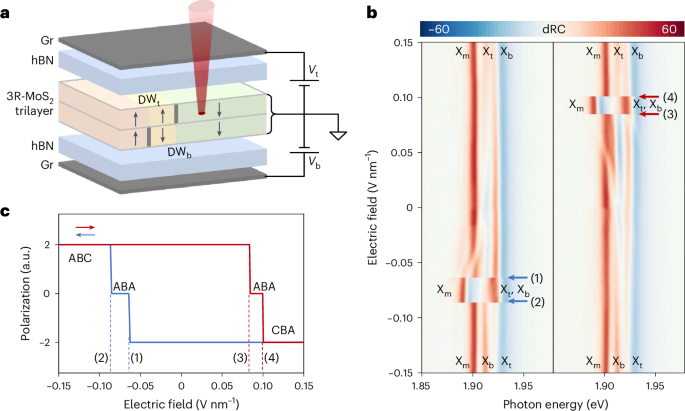
Unlike conventional ferroelectrics – where polarization reversal is achieved through the displacement of ions – sliding ferroelectricity in two-dimensional van der Waals materials emerges from the relative motion between atomic layers. In our work, we explore this unique mechanism in trilayer 3R‑ MoS2, where the polarization state is governed solely by the stacking order between adjacent layers. Under an applied electric field, the stacking configuration transforms from an initial state (for example, CBA) to a final state (ABC) via distinct intermediate states (ABA and BAB). One might assume that such subtle atomic-scale shifts could only be resolved by atomic-resolution electron microscopy; instead, our optical approach makes these transitions accessible. By employing reflection contrast spectroscopy at low temperatures, we observe spectral changes that serve as fingerprints for each stacking configuration, thus opening a window for revealing the interlayer dynamics.
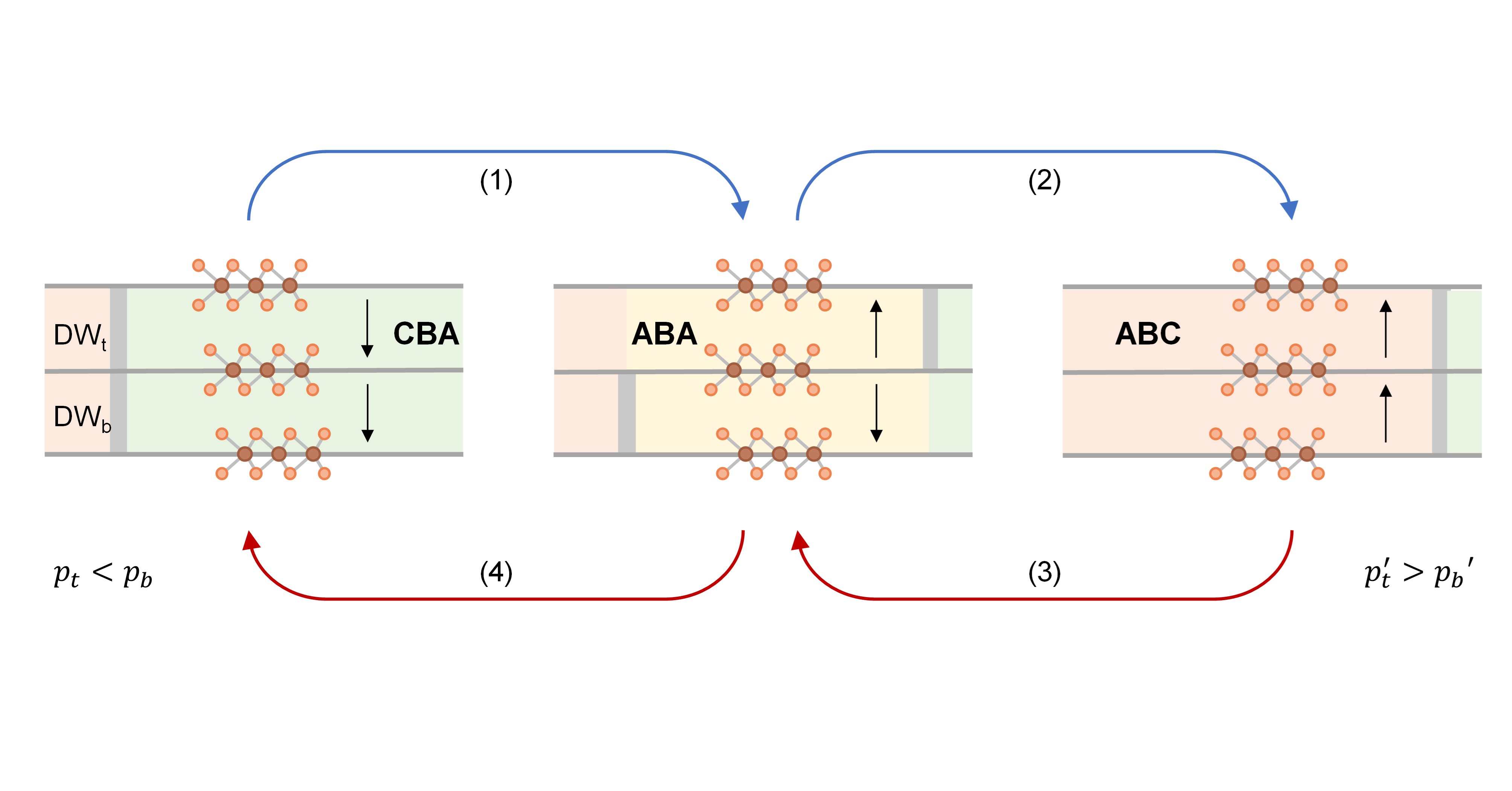
Our detailed investigations reveal that the polarization switching in 3R‑ MoS2 is not a simple, one-step process but rather a complex, multi-stage phenomenon (Figure 1). The transition is marked by a sequential unpinning of domain walls that separate regions of different polarization. Local defects, or pinning centers, play a critical role by anchoring domain walls at the top and bottom interfaces of the device, thereby dictating the order in which the layers undergo sliding. The distinct optical signatures of the intermediate ABA and BAB states – manifested as shifts in exciton energies and variations in oscillator strengths – allow us to map the entire switching pathway with precision, providing crucial insights into how atomic-scale movements are influenced by local imperfections.

Figure 1. Polarization switching in a 3R-MoS2 trilayer involving ABA stacking as the intermediate state.
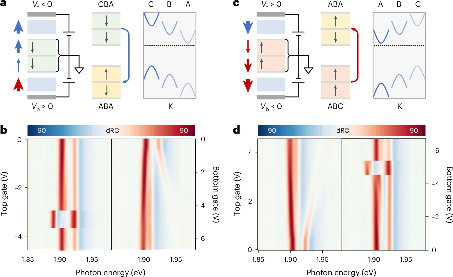
A particularly intriguing finding of our study is the asymmetric influence of the applied electric field (Figure 2). Our analysis reveals that n‑type doping in MoS2 leads to uneven free-carrier screening, so that the effective electric field experienced by the top and bottom interfaces differs. As a result, for a given polar state, only one electrode’s field may be sufficiently potent to drive the switching, triggering a stepwise release of domain walls. This asymmetry in field screening not only explains the observed sequential switching but also underscores the delicate balance between interlayer interactions, defect pinning, and electrostatic forces in determining the polarization dynamics.
In our Nature Nanotechnology paper, we detail these findings and discuss how this complex switching behavior could be harnessed to design multi-state devices for applications in memory, sensing, and computing. By combining precise optical spectroscopy with innovative device engineering, our work opens a new pathway for controlling and exploiting sliding ferroelectricity in two-dimensional materials.
Follow the Topic
-
Nature Nanotechnology
An interdisciplinary journal that publishes papers of the highest quality and significance in all areas of nanoscience and nanotechnology.


Please sign in or register for FREE
If you are a registered user on Research Communities by Springer Nature, please sign in