In the fast-paced world of photovoltaics, achieving higher energy conversion efficiency is both the goal and the challenge for solar cell researchers. Our recent paper, “27.09%-efficiency silicon heterojunction back contact solar cell and going beyond”, reflects our significant progress in this area by developing a new generation of heterojunction back contact (HBC) solar cells that not only push efficiency boundaries but also address key challenges in design and implementation.
The journey behind this paper was rooted in our desire to overcome fundamental limitations of conventional solar cell architectures. HBC solar cells have long been recognized as having enormous potential due to their ability to mitigate front-electrode shading losses and improve charge carrier collection efficiency. However, bringing this technology closer to its efficiency limits required addressing complex issues, particularly around charge carrier recombination and transport.
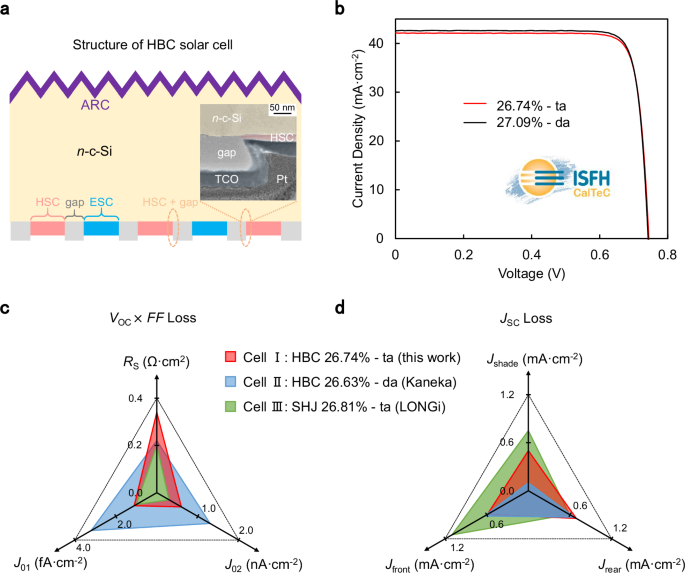
In this paper, we introduce our 27.09%-efficient HBC solar cell, certified by an independent testing institute (ISFH). But beyond reporting this new record-breaking efficiency, the paper dives deep into the underlying physics and challenges that had to be tackled, and proposes solutions for the next frontier of solar cell design.
The Story of Silicon Heterojunction Back Contact Solar Cells
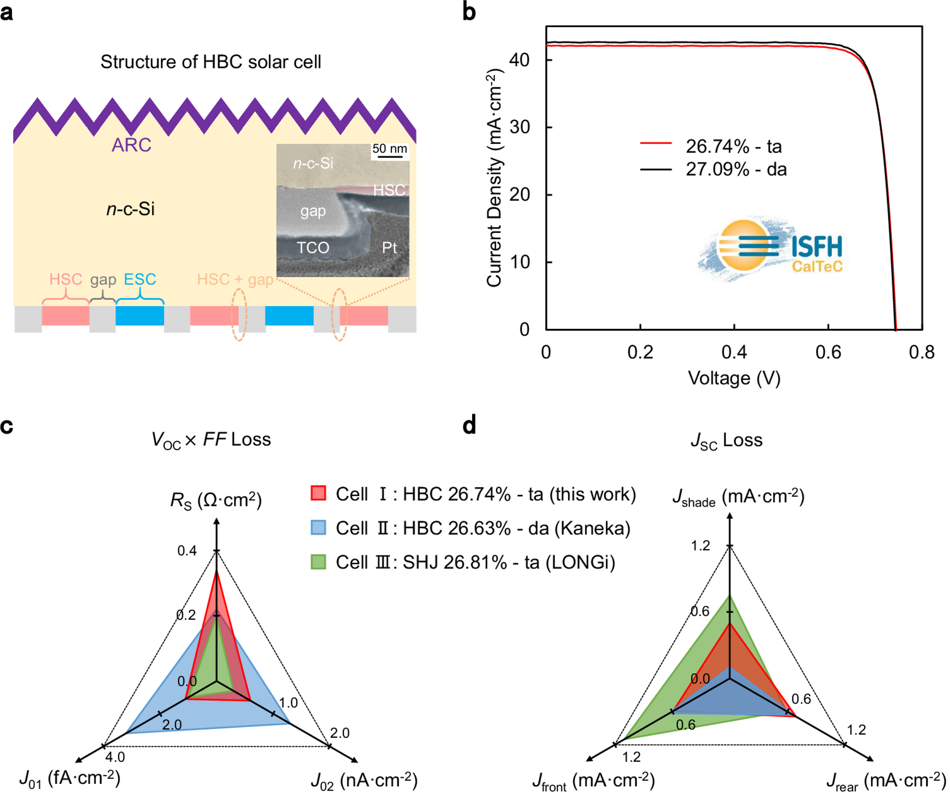
The development of silicon heterojunction solar cells has been crucial in advancing photovoltaic technology. These cells combine the best of two worlds: the crystalline silicon wafer, which provides the photovoltaic effect, and the amorphous silicon layers, which offer excellent passivation properties. Adding the interdigitated back contact (IBC) design, which places all metal contacts on the rear of the cell, allows for maximal light absorption with minimal front-surface interference.
However, even with this promising architecture, optimizing the performance of HBC solar cells involves significant challenges. Key issues that have hindered progress include:
1. Carrier Recombination: Unwanted recombination of charge carriers, especially at the hole-selective contact (HSC) and polarity boundaries, is a persistent problem.
2. Resistive Loss: High contact resistivity in both the hole-selective and electron-selective regions can lead to increased series resistance and lower overall efficiency.
3. Edge Effects: In many cases, the edge becomes a key channel for current density loss, as carriers that should be collected are instead lost to recombination.
Our team at Sun Yat-sen University and LONGi Green Energy has been working tirelessly to address these issues, developing a unique approach to solving them while maximizing the overall efficiency.
Addressing Carrier Recombination and Resistive Loss
One of the key findings of our research is that recombination losses primarily arise from the HSC region and the polarity boundaries between electron and hole contacts. To tackle this, we employed a combination of experimental and theoretical approaches to map out where recombination occurs and how it can be minimized.
We introduced advanced techniques for passivation, especially at the wafer edge, where current density loss is particularly pronounced. Once we successfully mitigated recombination around the electron-selective contact (ESC) region through electrical shading, the wafer edge itself became the primary source of loss. Thus, further improvements had to come from focusing on edge passivation technologies and refined surface treatments.
Additionally, by leveraging a laser ablation technique, we achieved a highly precise and clean separation of different contact regions on the rear of the cell. This contributed to reducing the contact resistivity and improving the series resistance (RS), leading to an overall enhancement in electrical performance. In this work, we managed to achieve an RS value of approximately 0.34 Ω·cm², a significant improvement but still leaving room for future optimization.
Performance Validation and Results
To validate the performance of our HBC solar cells, we employed a comprehensive set of tests and characterization techniques. Certified efficiency measurements at ISFH confirmed the 27.09% efficiency figure, a record that reflects both the electrical and optical improvements made during development.
Our analysis of recombination current density (J0) and resistive loss provides a clearer understanding of where further optimization is needed. For instance, the open-circuit voltage (VOC) achieved in this work was 745 mV, one of the highest reported for an HBC cell with a wafer thickness of 175 µm. This demonstrates the effectiveness of our passivation strategies, particularly in the HSC region, where recombination is most likely to occur.
We also found that improving the design of the rear reflector and optimizing the front anti-reflection coating were critical to achieving the overall efficiency gains. By meticulously balancing both the optical and electrical properties of the cell, we were able to enhance current density (JSC) and fill factor (FF), both of which contribute directly to the power conversion efficiency (PCE).
Looking Ahead: Toward 27.7% Efficiency and Beyond
While 27.09% is a significant achievement, our work outlines a clear path toward even higher efficiencies. We project that with further refinements in passivation techniques, particularly at the wafer edge, and by introducing more advanced nanocrystalline silicon contacts, it is possible to reach efficiencies of 27.7% or higher.
Nanocrystalline silicon offers superior contact properties compared to amorphous silicon, and its integration into the HSC and ESC regions could lead to even lower contact resistivity and improved carrier transport. Furthermore, improved wafer-edge passivation techniques, such as the application of thin layers of atomic-layer-deposited AlOx or organic passivation materials, could significantly reduce current density loss and further boost efficiency.
Our roadmap includes incorporating cutting-edge nanocrystalline silicon for both HSC and ESC regions, thereby reducing resistive losses to below 0.12 Ω·cm². Coupling this with advanced rear-side patterning and front-side anti-reflection coatings, we foresee pushing the efficiency limit of HBC cells closer to 28%.
A Collaborative Effort
This paper represents the culmination of many years of collaborative research between academic and industrial partners. Our partnership with LONGi Green Energy allowed us to leverage their expertise in mass production technologies and high-precision fabrication, while our research team at Sun Yat-sen University focused on addressing the fundamental scientific challenges.
Throughout the process, we have been driven by the knowledge that silicon photovoltaics remains the most scalable and cost-effective technology for global energy needs. Pushing the efficiency limits of silicon solar cells is essential if we are to meet the increasing global demand for clean, renewable energy.
Final Thoughts
Our work on high-efficiency HBC solar cells marks an important step forward in photovoltaic research. By addressing both electrical and optical limitations, and proposing a clear pathway for further efficiency improvements, we believe that the future of solar energy is bright.
While our 27.09%-efficient HBC solar cell sets a new standard, the pursuit of even higher efficiencies continues. Our research demonstrates that with the right combination of materials, technology, and design, it is possible to push the boundaries of what silicon solar cells can achieve. We look forward to continuing this journey and to seeing the impact of these advancements on the global solar energy landscape.


Please sign in or register for FREE
If you are a registered user on Research Communities by Springer Nature, please sign in