A bioinspired permeable junction approach for sustainable device microfabrication-Nature Sustainability
Published in Chemistry, Earth & Environment, and Materials

As one of the most crucial tools for neural communication, bioelectronic stimulator can effectively modulate neuron systems with electrical stimulation. However, personalizing the pattern of neural stimulators typically requires highly sophisticated tools, like photolithography, and facilities such as clean rooms. These methods are energy-intensive, generate hazardous chemicals, and demand significant time and expertise to operate.
One day, my advisor, Bozhi Tian, a professor, and talented artist at the University of Chicago, posed an intriguing question: What if we could directly write neural stimulators on substrates, much like traditional Chinese patterning? This imaginative idea not only redefines bioelectronics fabrication but also goes beyond the current achievements in the bioelectronics community. However, to realize this vision is not easy. We must address several challenges: improving the resolution of traditional brushes, developing suitable conductive ink, and achieving precise control with an automated writing platform.

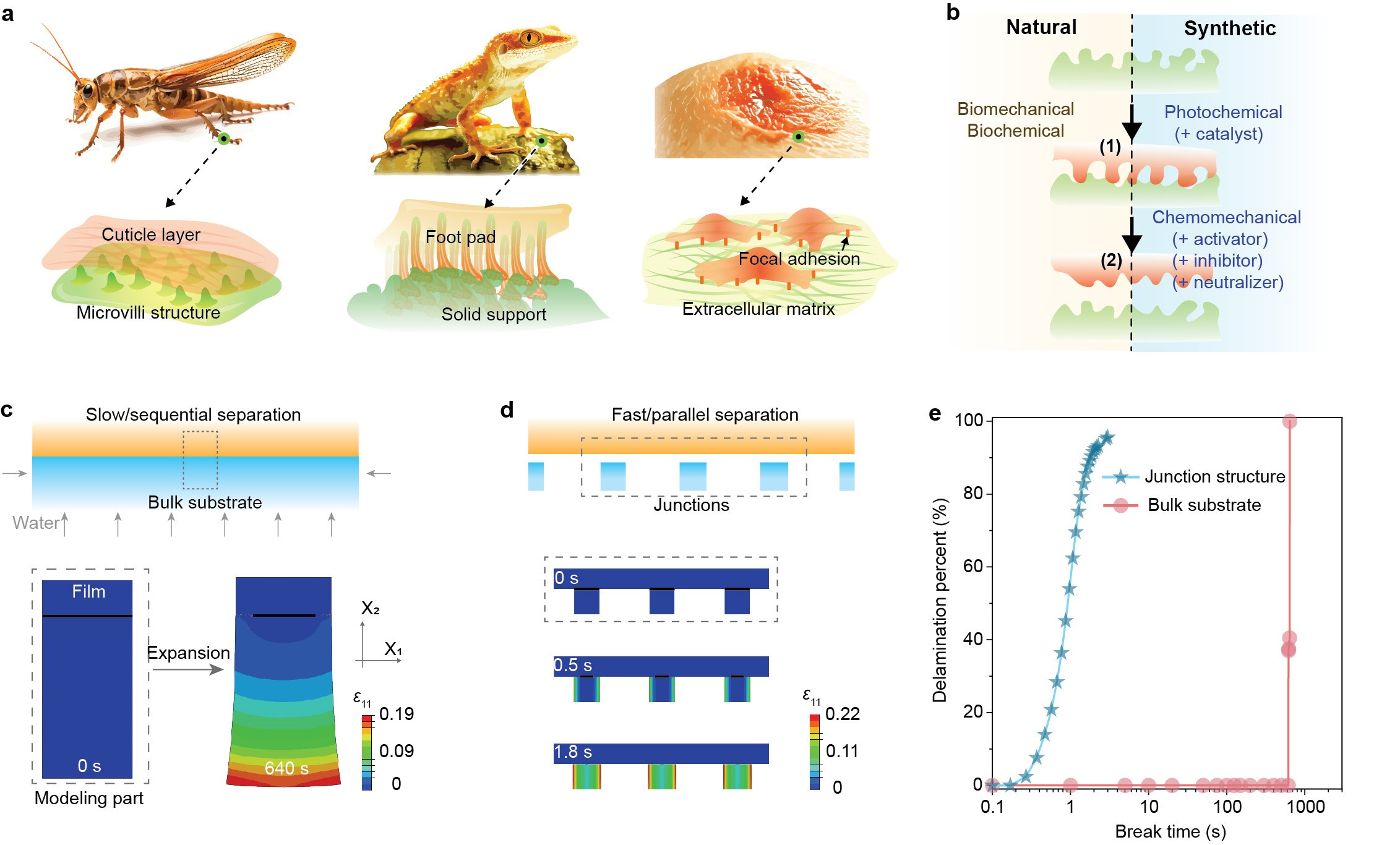
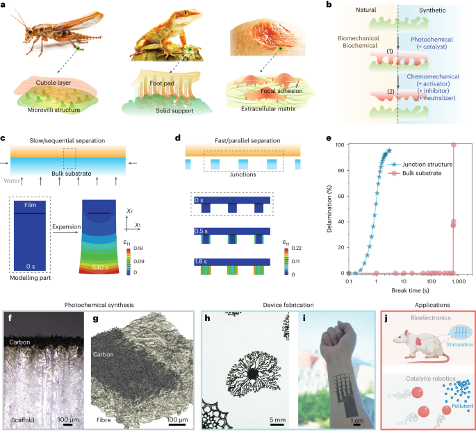
As we contemplated methods for electronics fabrication, the laser system in our lab caught my attention due to its high collimation, energy, and precise focus point. Traditionally, lasers have been used on polyimide, which is not suitable for paper and other substrates. Upon examining the mechanisms in these traditional methods, I discovered that the transformation mainly results from high-temperature induced localized pyrolysis. After thoroughly reviewing the literature on pyrolysis, I hypothesized that adding certain salts might facilitate the photochemical transformation of cellulose into carbon or graphene materials. Through experimentation, I identified several candidates perfect for surface patterning without the need for photolithography. This discovery was truly inspiring. Despite this breakthrough, achieving our initial goal of writing any pattern onto arbitrary surfaces remained challenging. Eventually, we found that using borate, a soluble salt that does not affect the cellulose structure, enabled the effective substrate swelling ad floating of patterns in water. This discovery reminded us of the famous poet John Keats, who wrote his epitaph: "Here lies one whose name was writ in water." This method is elegantly simple, which allows us to create and transfer delicate patterns on almost any substrate, paving the way for future bioelectronics applications. Moreover, this separation is ultrafast (<1s) on aerogel or paper, significantly outperforming traditional methods and also overcoming the longstanding issue in the field that typically requires harsh chemicals like HF or NMP.

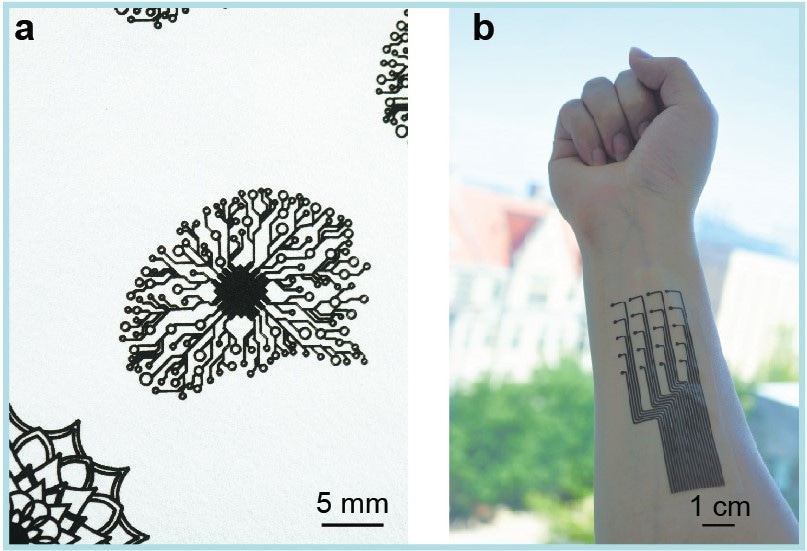
Figure 2. Images of fabricated neuron- and flower like devices on cellulose paper, and an EMG electrode array on PET attached to a human forearm through water-assisted transfer.
There appears to be a delicate balance between the structure and the delamination properties. Delving deeper into the mechanisms, we found a similarity between the microstructure of our substrates—whether aerogel or paper—and the footpads of geckos, which can adhere tightly to surfaces while moving swiftly when needed. In collaboration with Prof. Lihua Jin and Dr. Wei Chen from UCLA, we thoroughly calculated how the micropillar structure accelerates the delamination speed. Their calculations helped us visualize the separation process, which cannot be observed with experimental methodologies. Building on this method, we proposed using nanocellulose fibers for traditional microfabrication, significantly enhancing the delamination speed by approximately 1 order of magnitude. This structure-property relationship deepens our understanding of interfacial phenomena in microfabrication and subsequent processing. The universality of our platform also highlights its potential for generating devices with tailored properties for specific applications.

As we look to the future, manufacturing is evolving to be large-scale, intelligent, and carbon neutral. Collaborating closely with Dr. Aleksander Prominski, we developed a Roll-to-Roll apparatus in our lab, demonstrating the practicality of scaling up from small laboratory experiments to large-scale manufacturing production. This kind of transition from traditional batch processing represents the cutting edge of manufacturing. Simultaneously, the manufacturing sector must prioritize minimizing its carbon footprint throughout the life cycle. We integrated Life Cycle Assessment (LCA) into our work to quantify the environmental impact of representative systems. By digitalizing the flows of material, energy, and greenhouse gases, we comprehensively assessed the environmental impacts of various microfabrication techniques at different stages. Our paradigm holds significant potential for guiding carbon-neutral development across various sectors, including energy storage devices, sensors, flexible electronics, and robotics. This approach not only advances manufacturing technology but also aligns with the critical goal of sustainability.

For further readings, you are invited to read our complete paper, “A bioinspired permeable junction approach for sustainable device microfabrication”, published in Nature Sustainability: https://www.nature.com/articles/s41893-024-01389-5
Follow the Topic
-
Nature Sustainability
This journal publishes significant original research from a broad range of natural, social and engineering fields about sustainability, its policy dimensions and possible solutions.
Your space to connect: The Fuel cell technologies Hub
A new Communities’ space to connect, collaborate, and explore research on Electrochemistry, Chemical Engineering, and Fuel Cells!
Continue reading announcement


Please sign in or register for FREE
If you are a registered user on Research Communities by Springer Nature, please sign in