A fabrication process for flexible single-crystal perovskite devices
Published in Electrical & Electronic Engineering
In the past few years, hybrid perovskites have been widely developed into optoelectronic devices. Engineering high-quality polycrystalline thin films is rapidly pushing the device's performance. However, the researches based on single-crystal perovskite devices are still under a preliminary status. The basic fabrication of single-crystal hybrid perovskites with suitable thickness, area, and composition, are still challenging.
To address the issue of precise controls on the crystal thickness, size, and composition simultaneously, we report a solution-based lithography-assisted epitaxial-growth-and-transfer method for fabricating general perovskite-based devices with single-crystal materials on arbitrary substrates. Leveraging our unique controlled epitaxial growth, single-crystal devices have been demonstrated with not only high stabilities but also good performance.
In our study, a solution-based growth method is adopted to epitaxially grow the single-crystal hybrid perovskites, and a designed pattern mask is critical for realizing the formation of thin films and their thickness control. Also, by using a more rigid mask, scaled fabrication on single-crystal micro-dots or thin films are feasible. Furthermore, the orientation control is also achieved and integrated into functional devices, allowing a specific design of the crystal morphology with desirable functionalities. Based on this method, single-crystal hybrid perovskite-based micro-light-emitting diodes, antireflective photodetectors, and photovoltaics are demonstrated, showing their wide applications.

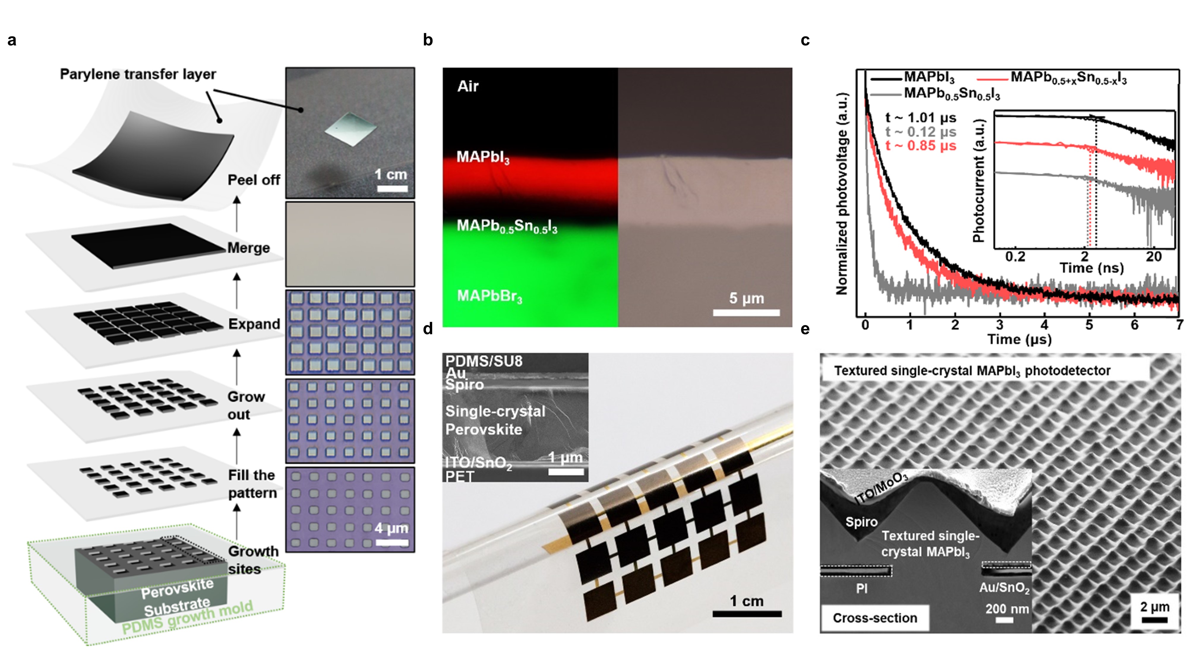
Figure. Work summary. a, Schematics (left) and corresponding optical images (right) showing the solution-based epitaxial growth, merging and transferring processes of the single-crystal perovskite thin film. The bottom four optical images share the same scale bar, 4 μm. b, A photoluminescent image (left) of the graded single-crystal MAPb0.5+xSn0.5−xI3 grown on a MAPbBr3 substrate. The dark tin-rich area is because of the infrared emission of the tin-alloyed MAPbI3 being invisible on the camera. A corresponding optical image (right) shows the graded MAPb0.5+xSn0.5−xI3 without noticeable structural interfaces. c, Transient photovoltage measurements show that the graded single-crystal MAPb0.5+xSn0.5−xI3 shows a relatively long carrier lifetime due to the easier exciton separation and charged carrier collection facilitated by the graded bandgap. Inset: Time-of-Flight measurements show that the carrier mobility in graded single-crystal MAPb0.5+xSn0.5−xI3 is close to that in the compositionally uniform single-crystal MAPb0.5Sn0.5I3. The inflection points of the photocurrent curves are marked by the dotted lines. d, An optical image showing an array of flexible single-crystal photovoltaic islands with a total working area of 6.25 cm2 (0.5 cm × 0.5 cm × 25). Inset: a cross-sectional scanning electron microscopy image of the single-crystal perovskite photovoltaic device. e, Scanning electron microscopy images showing the textured single-crystal MAPbI3 thin film as a photodetector. Inset: a magnified image of the cross-sectional structure of the device. PI, polyimide.
It has also been found that an ultra-thin thickness of the single crystal is able to dramatically enhance its flexibility. A neutral mechanical plane design is adopted to realize the flexible single-crystal hybrid perovskite devices. The as-demonstrated devices exhibit promising flexibility and stability against bending. In addition, further integration within an island-bridge network exhibits even improved robustness.
Besides, we also find that continuously exchanging the components of the growth solution can result in composite-graded single-crystal perovskites along the growth direction, which forms a graded bandgap in such a single crystal. The graded bandgap without any physical interfaces helps suppress the carrier recombination and prolong the carrier lifetime, resulting in more efficient charge separation and collection.
Finally, flexible single-crystal hybrid perovskite photovoltaics based on lead-tin gradient alloying are demonstrated with a largely enhanced open-circuit voltage, leading an improved power conversion efficiency. It will be expected that this method for fabricating single-crystal perovskite devices may open up more opportunities to explore this class of fascinating materials and hold promises for realizing high-performance single-crystal perovskite electronics.
Nevertheless, further developments and studies are needed to improve the fabrication yield and interfacial conditions. Also, the dependence of the substrate may finally become the bottleneck for addressing the scalability issue with industrial requirements. Further optimized technics and/or new substrates will be needed.
Follow the Topic
-
Nature
A weekly international journal publishing the finest peer-reviewed research in all fields of science and technology on the basis of its originality, importance, interdisciplinary interest, timeliness, accessibility, elegance and surprising conclusions.


Please sign in or register for FREE
If you are a registered user on Research Communities by Springer Nature, please sign in