A highly CMOS compatible hafnia-based ferroelectric diode
Published in Electrical & Electronic Engineering

Computing systems use a hierarchy of volatile and non-volatile data storage devices to achieve an optimal trade-off between cost and performance. However, the frequent data transfer between different memories leads to the decreased bandwidth and degraded computing efficiency, especially in the case of massive data computing, resulting in the well-known ‘memory wall’ issue. To effectively solve the memory wall problem, a desired way is to configure a memory with high speed and high density features.
Among various non-volatile memories, ferroelectric random access memories (FeRAM), which achieve non-volatility by switching and sensing the polarization state of a ferroelectric capacitor, were thought as an ideal memory solution due to their outstanding features of low power, high speed, high endurance and good retention. However, the scaling limitation of perovskite ferroelectric materials hindered it from wide applications. The development of FeRAM in semiconductor industry has been stopped at 130 nm node for a long time. The discovery of ferroelectricity in doped HfO2 has renewed the interest in ferroelectric memory by offering a possible solution to bridge the scaling gap between perovskite ferroelectric materials and CMOS technology.
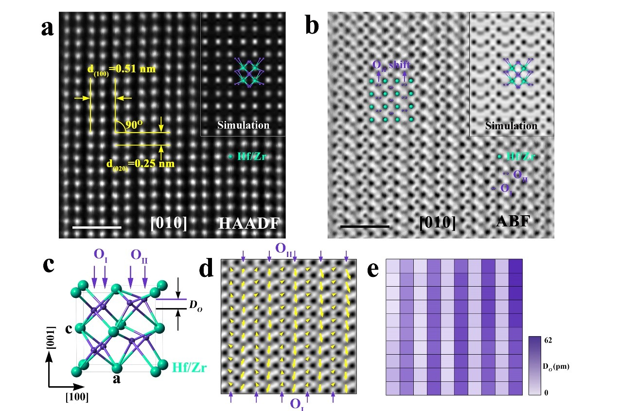
The structural origin of the ferroelectricity in HfO2 based materials was hypothesized to be the formation of the noncentrosymmetric orthorhombic phase. There are four different space groups in o-phase, i.e., Pca21, Pbcm, Pmn21 and Pbca. The Pmn21 phase could be easily ruled out by the image of the hafnium sublattice. However, distinguishing between the Pbca, Pbcm, and Pca21 space groups is quite challenging, which could be only realized by visualizing the tiny difference of oxygen sublattice. In this work we (researchers from IMECAS and East China Normal University) unambiguously identified the Pca21 phase in HZO film by visualizing both the hafnium/zirconium lattice order and oxygen lattice order with atomic-resolution spherical aberration (Cs)-corrected STEM (Figure 1).

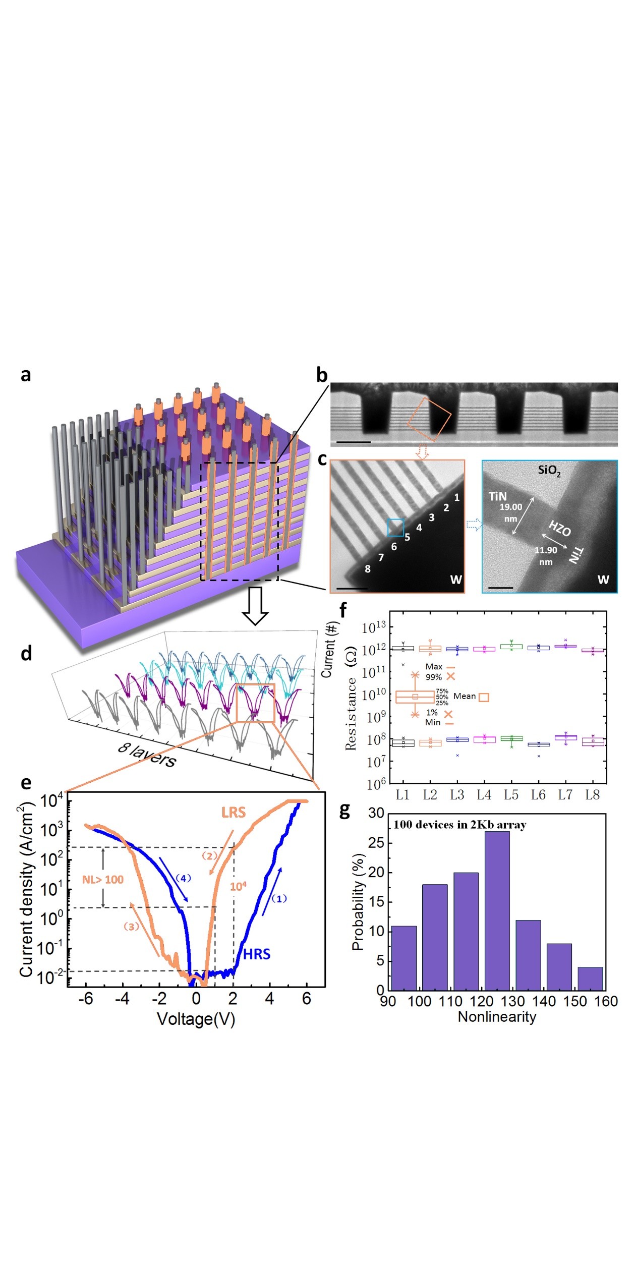
Up to now, ferroelectric HfO2 based memories in forms of 1T1C and FeFET structures have been demonstrated. The 1T1C FeRAM requires large capacitor area and undergoes destructive read out. FeFET can realize non-distructive read and 3D vertical stack. However, it cannot be used as a random access memory. Two terminal devices such as FTJ and Fe-diode have the potential to achieve high density crossbar array. The tunnel electroresistance effect of FTJ was generally formulated by quantum mechanical electron tunneling mechanism. In principle, both the on and off states of FTJ obey linear or quasi-linear I-V relationship, which makes it need extra selector device to diminish the sneaking current in crossbar array. In contrast, the Fe-diode, with the working principle governed by Schottky barrier modulation as polarization reversal, has the potential to gain inherent nonliearity and realize selector-free crosspoint integration. Fe-diode composed by conventional perovskite materials such as PbTiO3, BiFeO3 and Pb(Zr,Ti)O3 were commonly reported. However, low readout currents and low on/off ratio limited their miniaturization. Based on HfO2 ferroelectric material, we further demonstrated a fully CMOS compatible ferroelectric diode with high readout current density (>200 A/cm2) and build-in nonlinearity (>100), which was implemented to three-dimensional integration up to 8 layers with vertical size down to 20 nm (Figure 2).

Follow the Topic
-
Nature Communications

An open access, multidisciplinary journal dedicated to publishing high-quality research in all areas of the biological, health, physical, chemical and Earth sciences.
Related Collections
With Collections, you can get published faster and increase your visibility.
Women's Health
Publishing Model: Hybrid
Deadline: Ongoing
Advances in neurodegenerative diseases
Publishing Model: Hybrid
Deadline: Mar 24, 2026


Please sign in or register for FREE
If you are a registered user on Research Communities by Springer Nature, please sign in