AI-Assisted Acoustic Interferometry - New Possibilities for Failure Analysis of 3D Interconnect Technologies
Published in Electrical & Electronic Engineering
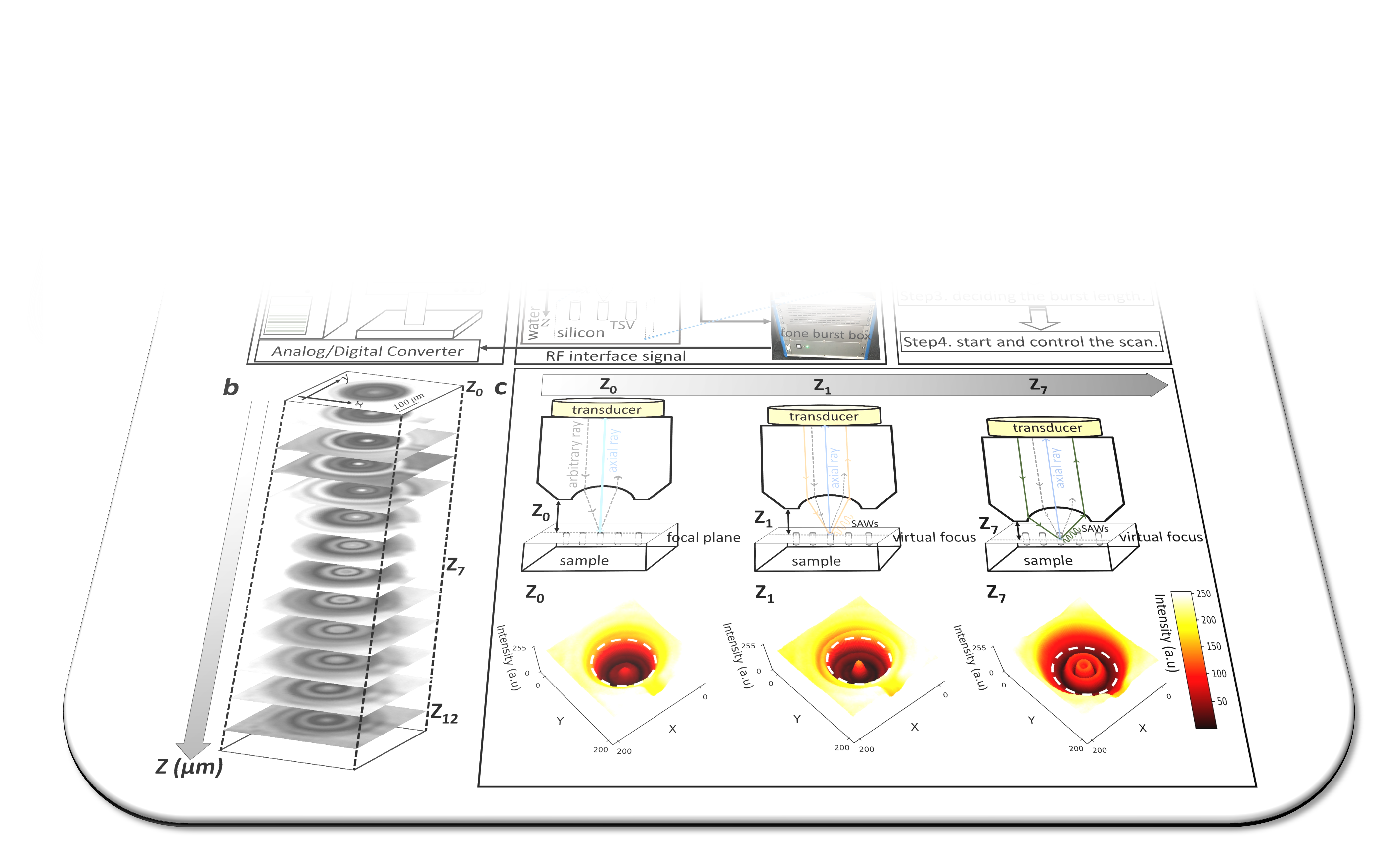
3D integration technology in the field of microelectronics helps to configure highly integrated heterogeneous devices by vertically stacking different functional components together with a notably reduced form factor. 3D integration technology addresses the convergence of Moore’s law and More than Moore (MtM). In this context so-called through silicon vias (TSVs) are utilized to build sophisticated and multifunctional microelectronic setups like microelectromechanical systems (MEMS), inductors, power electronics, optical sensors, and 3D packages with low cost and miniature size. TSVs are either filled or coated with a conductive metal, leading to the so-called filled or open TSV technology respectively. However, emerging residual stress may cause critical damage formation such as delamination and/or cracks in the sidewall or bottom of the TSV. Therefore, defect detection in TSVs on micron-level and below is crucial to ensure the quality of interconnects in the production.
Nevertheless, the in-line failure analysis within an industrial environment of TSVs poses a tremendous challenge. In particular, the requirement such as the non-destructive high-resolution characterization of defects with micron- and sub-micron size in a time and cost-efficient manner, and to gain a statistical relevant amount of TSVs on wafer level in-line, is very tough to fulfill.
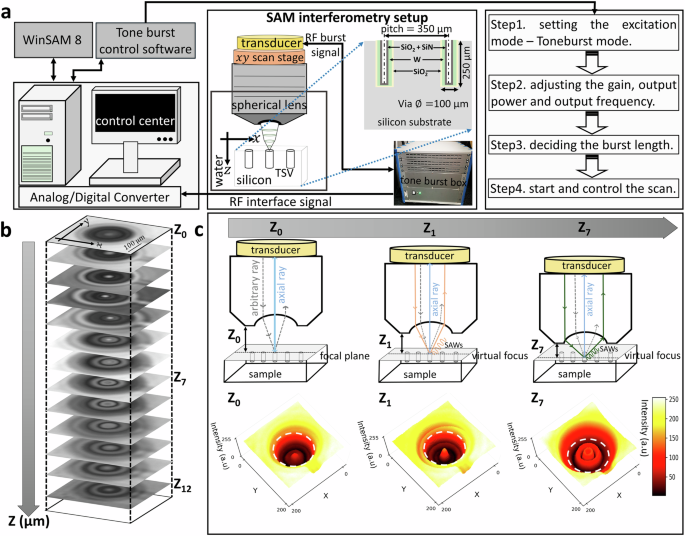
A team of scientists within the group Brunner at MCL as well as industrial partners applied the concept of acoustic interferometry for cost and time efficient high-resolution failure analysis in TSVs down to the nanometer regime. Modified transducers utilized within a highly industrial serviceable scanning acoustic microscope setup are capable to excite surface acoustic waves .
In particular, the team uses customized transducers with a central frequency of 100 MHz and lenses with wider opening angle, exceeding the critical Rayleigh angle and enabling the controlled excitation of Rayleigh waves or surface acoustic waves (SAWs).
They conduct, accompanied to the experimental results, wave propagation simulations based on elastodynamic finite integration technique (EFIT) to validate the generation of SAWs utilizing the SAM interferometry setup on wafer level as well as to contribute to a deeper understanding of SAW propagation, with a specific focus on the angles of the acoustic lenses.
Differently detected SAM interference patterns could be associated in an automated manner by utilizing an end-to-end convolutional neural network to either non-defective or various defective TSV classes.

The presented methodology shows that the controlled excitation of surface acoustic waves facilitates the detection of nm-sized cracks, an essential accomplishment for modern failure analysis in 3D integration technologies. The team points out that the discussed acoustic interference approach is not only limited to failure analysis of TSVs but can be also exploited to further topics.
Follow the Topic
-
Communications Engineering
A selective open access journal from Nature Portfolio publishing high-quality research, reviews and commentary in all areas of engineering.
Related Collections
With Collections, you can get published faster and increase your visibility.
Engineering the future of 2D transistors: scaling, p-doping, and contact strategies
Publishing Model: Open Access
Deadline: May 31, 2026
Microgrids and Distributed Energy Systems
Publishing Model: Hybrid
Deadline: Jun 30, 2026




Please sign in or register for FREE
If you are a registered user on Research Communities by Springer Nature, please sign in