With the continuous advancement of the semiconductor industry, electronic devices are constantly developing towards miniaturization and integration. A small chip, viewed 10,000 times larger under a microscope, is no less complex than a city. For example, the iphone12 is equipped with a 5-nanometer process mobile phone processor, Apple A14, which integrates 11.8 billion transistors, and the size of the processor is not much bigger than a fingernail. For such highly integrated devices, in order for these nano structures with such small intervals to work together and without interference, the boundary between the two must be "angular". However, there are still challenges for traditional chemical vapor deposition (CVD) and physical vapor deposition (PVD) to achieve efficient and precise controlled deposition of complex structures at such a tiny scale. The research group of Professor Rong Chen and co-workers from Huazhong University of Science and Technology obtained a self-aligned patterning of a dielectric oxide film larger than 5nm on SiO2 with no observable growth in the Cu region on a Cu/SiO2 nanopattern structure. The technology can "build" the structure with atoms like Lego bricks, so that more complex structure can be made with high precision, and also to meet the market demand for miniaturization in the field of integrated circuits.
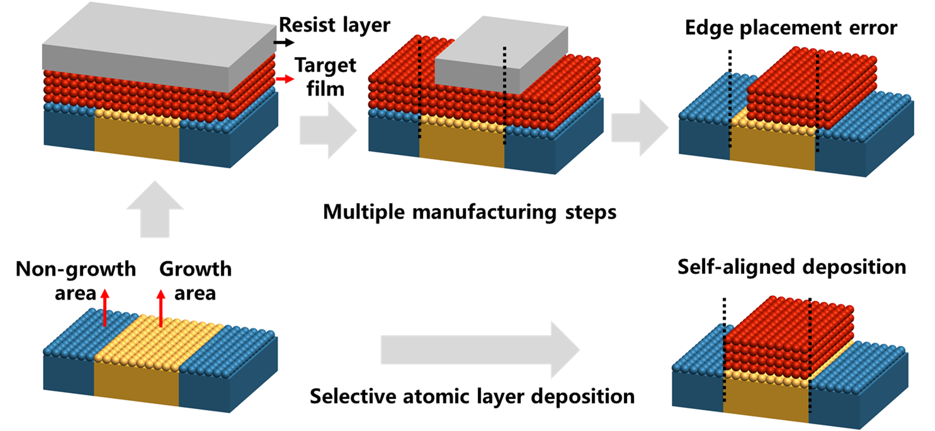
The semiconductor industry continues to develop smaller, better performing nano-electronic devices; High resolution patterning is a key step in determining the manufacturability of such devices. Stacking errors hinder high-precision patterning because nanodevices tend to shrink to the atomic scale. The traditional top-down "deposition-lithograph-etching" multiple manufacturing steps are limited by significant challenges, such as the control of edge placement errors (EPE) and the complexity of the steps (Figure 1). In addition, new materials and 3D nanostructures have stringent requirements for high-volume manufacturing (HVM) technology. With the reduction of the feature size of semiconductor devices and the increase of the number of stacked layers, the manufacturing of high precision limited region patterned films is becoming more and more urgent. Atomic layer deposition (ALD) is an important preparation method for atomic films. As early as 1998, atomic layer deposition began to be applied to non-volatile memory. By 2007, atomic layer deposition technology was used in the high dielectric/metal gate structure of Intel's 45 nm chips. The atomic layer deposition technique is based on a two-and-a-half reaction process of alternating exposure of precursor and co-reactant, molecular monolayer adsorption and reaction, thereby achieving self-limiting layer-by-layer surface deposition and atomic-level film thickness control.
 Figure 1: two routes for deposition of patterned films on a predefined patterned surface, where selective deposition of atoms on desired location is able to reduce the complex steps of material removal and enables high precision self-alignment
Selective ALD is a promising technique because it allows the atomic-scale precision alignment with simplified steps. Selective ALD enables deposition of films only on the desired regions of pre-patterned substrates. Selective ALD between dielectric oxides and metals is achieved through surface passivation. Polymers, self-assembled monolayers (SAMs), and small molecule inhibitors have been used to block nucleation in non-growth areas. These inhibitors assisted selective ALD methods are close to practical industrial applications, but challenges still exist. This process requires a long immersion time and subsequent removal of SAMs or inhibitors. Moreover, severe limitations exist because the blocking effect of SAMs deteriorates during the deposition process and is heavily temperature-dependent. As the critical size decreases below 10 nm and the demand for new materials and 3D nanostructures continue to increase, the appropriate chemicals for passivation-assisted selective ALD become limited. Inherently selective ALD is a developing, a more straightforward method for alignment manufacturing, that is free of inhibitor passivation and removal steps. In particular, ALD relies on intrinsic surface chemistry differences. Selective deposition of dielectric on dielectric is challenging to suppress nucleation on metals while ensuring deposition on dielectrics. This process is vital for Full Self Aligned Via (FSAV) fabrication in the Back end of line (BEOL) process becasue it increases the spacing between vias and metal lines.
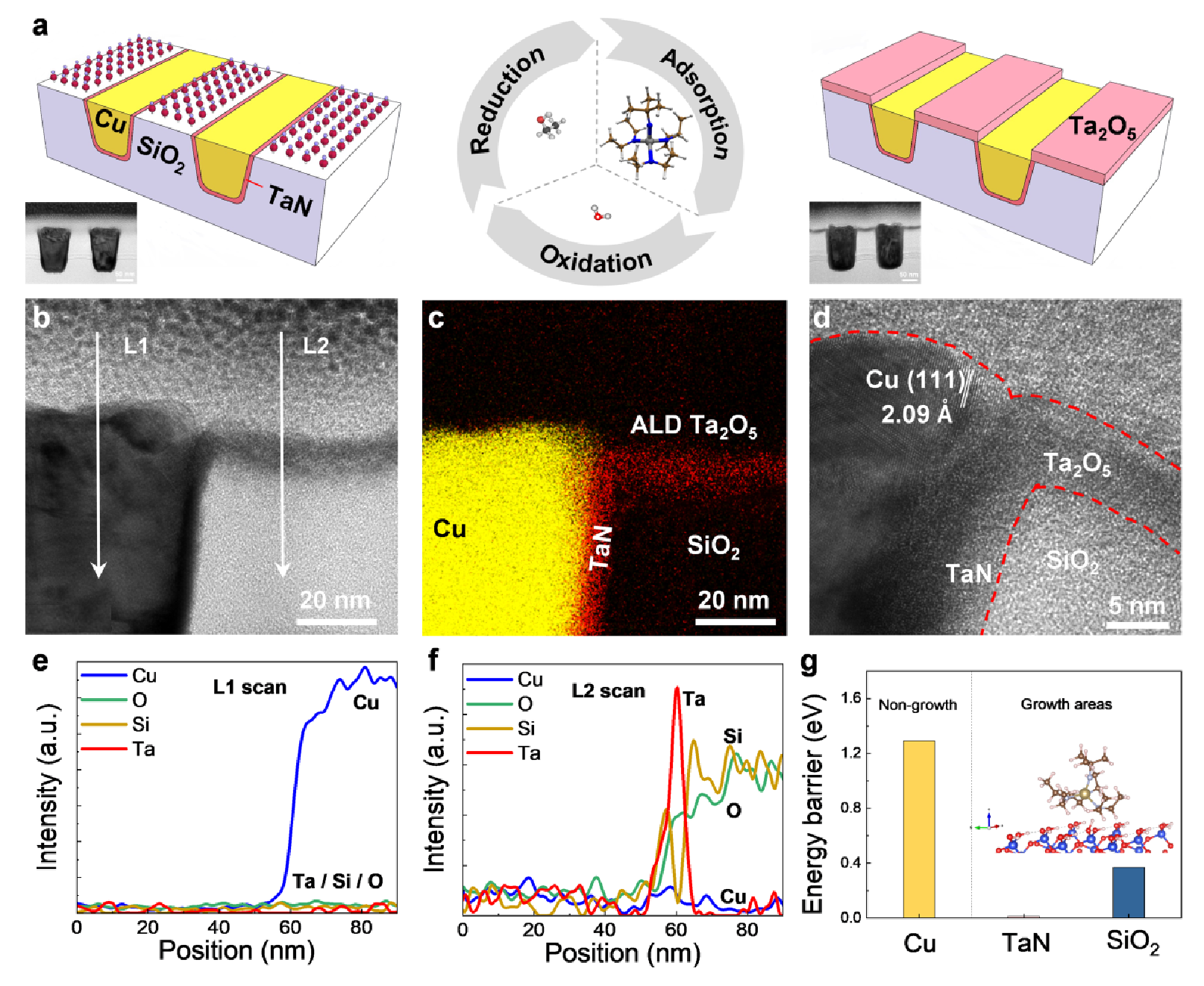
In this context, a redox-coupled inherently selective atomic layer deposition (ALD) is introduced to tackle this challenge. The ‘reduction-adsorption-oxidation’ ALD cycles are designed by adding an in-situ reduction step, effectively inhibiting nucleation on Cu. TaOx is selectively deposited on SiO2 before Cu for self-alignment applications. During the inherently selective ALD process, Ta(NtBU)(NEt2)3 is used as the Ta precursor, and chemicals such as reductant (EtOH), etchant (HAc), and oxidant (H2O, O2, and O3) are used as co-reactants. The Ta(NtBu)(NEt2)3 precursor has a higher energy barrier on reduced Cu surface than that of OH-terminated SiO2 surface, which is the origin of the ALD selectivity. The selectivity decreases with the oxidation of Cu during ALD. Optimized selectivity is achieved with redox-coupled ABC-type (EtOH-Ta(NtBu)(NEt2)3-H2O) ALD process, and EtOH is used to reduce the surface oxidation of Cu in situ. Moreover, the inherently selective ALD process is successfully transferred onto Cu/SiO2 nanopatterns with ~100 nm pitch and obtains high selectivity with more than 5 nm films on SiO2, and avoids excessive mushroom growth at the edges or the emergence of undesired nucleation defects within the Cu region. (Figure 2). The results indicate that inherently selective ALD is a robust tool and offer a streamlined and highly precise self-aligned manufacturing technique, which is advantageous for the future downscaling of integrated circuits.

Figure 2: the scheme and TEM image of original 50 nm critical dimension Cu/SiO2 patterns and self-aligned patterning of TaOx film after redox-coupled inherently selective ALD.
If you want to know more about our work, please access the full paper in Communication Physics here: Self-Aligned Patterning of Tantalum Oxide on Cu/SiO2 through Redox-coupled Inherently Selective Atomic Layer Deposition
Follow the Topic
-
Nature Communications

An open access, multidisciplinary journal dedicated to publishing high-quality research in all areas of the biological, health, physical, chemical and Earth sciences.
Related Collections
With Collections, you can get published faster and increase your visibility.
Women's Health
Publishing Model: Hybrid
Deadline: Ongoing
Biosensing
Publishing Model: Hybrid
Deadline: Jun 30, 2026


Please sign in or register for FREE
If you are a registered user on Research Communities by Springer Nature, please sign in