Most scientists are introduced to halide perovskites through applications such as solar cells and LEDs. These materials have proved brilliant at absorbing and emitting light, and they can be made cheaply and easily. Now, we are discovering that these common materials hide a secret quantum life, coming into existence and vanishing faster than previously thought possible.
In a new study published in Nature Nanotechnology, we have discovered that bulk thin films of the hybrid perovskite formamidinium lead iodide (FAPbI3) can produce ultrafast quantum emissions on a scale of mere picoseconds (trillionths of a second). This discovery, which leverages intrinsic structural quirks of the material, rather than expensive engineering, could open new doors for quantum technologies.
The Quest for Faster Quantum Emission
Quantum emitters are the heart of technologies like quantum computing and ultra-secure communication. Ideally, they need to produce single photons of light (the smallest possible packet of light) and do it incredibly fast. Until now, achieving such ultrafast speeds has largely been the domain of complex, meticulously grown materials like gallium arsenide (GaAs), created in multi-million-dollar vacuum chambers.
Perovskites offered a tantalizing alternative. In 2020, (https://www.nature.com/articles/s41563-020-0774-9#Sec11) reported strange, sharp peaks in the light absorbed and emitted by films of formamidinium lead iodide (FAPbI₃) at extremely cold temperatures. These peaks appeared to be a signature of quantum confinement—where electrons are trapped in tiny structures, forcing them to behave like quantum particles. But the origin of these features and, crucially, how fast they operated remained a mystery.
A Multimodal Microscope Detective Story
To investigate this mystery, we had to use a suite of advanced tools to correlate the perovskite’s local crystal structure with its light-absorbing & emitting behaviour.
Catching the Blink: Ultrafast Spectroscopy
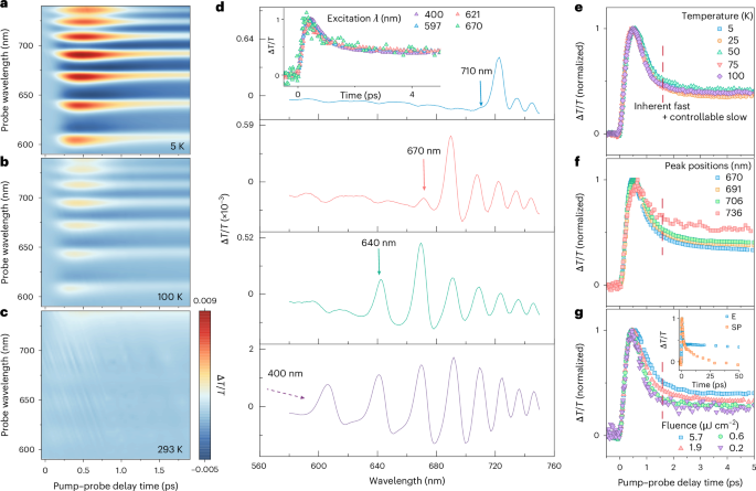
First, we use a technique called transient absorption spectroscopy (TAS). Think of it as a super-slow-motion camera for light absorption. During TAS, a sample is excited with an ultrafast "pump" of laser light , before being probed it with a second pulse. We then use these two pulses to understand how the material changed due to photoexcitation.
When using TAS, what we observed continued to surprise us. At cryogenic temperatures, the FAPbI3 film exhibited distinct energy levels that decayed away—"blinked out”—on a timescale of about 2 picoseconds. That’s orders of magnitude faster than typical light emission in these materials andwas the first evidence of ultrafast quantum transients.
Pinpoints of Perfect Light: Hyperspectral Imaging
Next, we mapped where the light was originating from spatially using a hyperspectral microscope. Unlike typical images, which are formed from a combination of red, green and blue colour channels; hyperspectral imaging provides an entire spectrum of light at each pixel. When we examined cryogenic-FAPbI3 using this microscope, instead of a uniform glow, we found that the emission came from tiny, isolated spots randomly scattered across the film, each acting like an independent, miniature lighthouse.
Even more impressive, the light from each spot was incredibly color pure, with an ultra-narrow linewidth. This lack of "blurriness" is a hallmark of a well-defined quantum state and ruled out other explanations like lasing.
The Structural Origin: Ubiquitous Nanotwins
The big question remained: what was causing this in the structure? We turned to a cutting-edge electron microscopy technique called 4D-STEM (scanning electron diffraction). This allowed us to create nanoscale maps of the crystal structure.
We discovered that the films were filled with a ubiquitous defect: nanoscale twins. On either side of the twin boundary the atoms in the crystal structure are mirrored, similarly to how a pair of gloves can be laid over each other palm-to-palm, and are also mirror images of each other. , . In FAPbI3, these twin boundaries represent layers where the fundamental building blocks of the structure (lead iodide octahedra) switch from sharing corners to sharing faces. This creates a different atomic environment at the boundary which we believe is crucial to understanding the quantum effects observed at cryogenic temperatures. We propose these defects can form an assembly of face and corner sharing octahedra called a superlattice, which when periodic will result in bright emission.
The Quantum Model: A Natural Superlattice?
We hypothesize this natural superlattice acts analogously like the artificial ones painstakingly grown in III-V materials. The corner-sharing regions act as quantum wells (boxes that trap electrons), while the face-sharing layers act as barriers.
Using a fundamental quantum mechanics model (the Krönig-Penney model), we showed that the width of these wells directly determines the energy (colour) of the emitted light. Whilst the ultrafast, ~2 ps decay is explained by another quantum phenomenon: tunneling. Due to how thin the barrier layers are the excited electrons do not have to climb over them but can tunnel through the barriers almost instantly instead, a process described by the Wentzel–Kramers–Brillouin (WKB) approximation, another cornerstone of quantum theory.
Why This Matters: A New Path for Quantum Materials
This work is significant for several reasons:
- It’s Intrinsic: The quantum behaviour comes from the material’s innate structure, not expensive external engineering. This makes it a cheap and scalable platform.
- It’s Ultrafast: Picosecond operation is crucial for high-speed quantum applications.
It’s a Blueprint: The multimodal approach—correlating ultrafast optics with nanoscale imaging—provides a powerful blueprint for discovering quantum phenomena in other complex materials.
The challenge and opportunity ahead lie in learning to control this nanotwinning. The question remains— can we grow these superlattices with perfect periodicity to get uniform, predictable quantum emission? If so, it could enable new designs for quantum light sources integrated directly into easy-to-make perovskite films, blending the quantum and classical worlds in a way that was previously unimaginable.
The full paper, "Picosecond Quantum Transients in Halide Perovskite Nanodomain Superlattices," is published in Nature Nanotechnology.
Follow the Topic
-
Nature Nanotechnology
An interdisciplinary journal that publishes papers of the highest quality and significance in all areas of nanoscience and nanotechnology.


Please sign in or register for FREE
If you are a registered user on Research Communities by Springer Nature, please sign in