Control of electronic band profiles through depletion layer engineering in core-shell nanocrystals
Published in Materials
Michele Ghini, Italian Institute of Technology
Written by Michele Ghini, Nicola Curreli, Ilka Kriegel.
Doped metal oxide (MO) nanocrystals (NCs) are gaining the attention of the scientific community thanks to the combination of unique properties, such as high electron mobility, the tunability of their carrier density, chemical stability, and low toxicity, as well as suitable operating temperature, which makes them appropriate for a large plethora of applications, ranging from nanoelectronics and plasmonics to the next-generation energy storage. In MO NCs, Fermi level pinning results into the formation of electronically depleted layers, which affect their optical and electronic properties. For precise control over functionality, it is important to understand the role of several structural and electronic parameters, with the aim to engineer the NC’s electronic band profiles at the nanoscale.
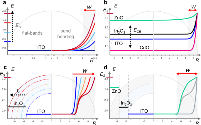
 and the energy in the ordinate (in eV). In each panel, the left side of the sphere represents the flat-band potentials in the non-equilibrium condition, while the right side reports the band bending due to the Fermi level pinning. Band profiles were calculated by numerically solving the Poisson’s equation. a, Tuning of surface state potentials (E_S). Increasing the E_S results in the expansion of the depletion width, W. b, Impact of different materials on W at fixed E_S. c, Expansion of W and double bending of the depletion layer in a core-shell structure of ITO-In2O3 with a core radius (R_core) of 5.5 nm and varying shell thickness. d, Multiple shell system by combining an ITO core (R_core= 5.5 nm) with a In2O3 and ZnO shell with total radius R = 9.5 nm. The band shows a complex profile with a triple bending (green curve). The grey curves illustrate the previously reported case of a uniform ITO NC (dark grey) and an ITO-In2O3 core-shell NC (light grey) with total radius R = 9.5 nm for comparison.")
Figure 1 | Depletion layer engineering of metal oxide NCs via tuning of structural and electrical properties. The morphology of the NC is illustrated by a semi-circle with its extension R in the abscissa (in nm) and the energy in the ordinate (in eV). In each panel, the left side of the sphere represents the flat-band potentials in the non-equilibrium condition, while the right side reports the band bending due to the Fermi level pinning. Band profiles were calculated by numerically solving the Poisson’s equation. a, Tuning of surface state potentials (ES). Increasing the ES results in the expansion of the depletion width, W. b, Impact of different materials on W at fixed ES. c, Expansion of W and double bending of the depletion layer in a core-shell structure of ITO-In2O3 with a core radius (Rcore) of 5.5 nm and varying shell thickness. d, Multiple shell system by combining an ITO core (Rcore = 5.5 nm) with a In2O3 and ZnO shell with total radius R = 9.5 nm. The band shows a complex profile with a triple bending (green curve). The grey curves illustrate the previously reported case of a uniform ITO NC (dark grey) and an ITO-In2O3 core-shell NC (light grey) with total radius R = 9.5 nm for comparison.
Our research group, led by Dr. I. Kriegel at the Italian Institute of Technology, investigated the impact of depletion layers on doped model oxide NCs (Figure 1). For instance, the presence of surface states and the combination of various materials and doping levels in diverse architectures lead to different energy band profiles and depletion layer widths. Exemplified by the case study of ITO-In2O3 core-shell NCs, we show that the introduction of more than one electronic interface induces a double bending of the energy bands accompanied by a distinct carrier density profile and multi-modal plasmonic responses. This induces a multiple bending within the nanoparticle effectively separating the NC into three distinct electronic regions: an active core region with specific carrier density, a transition region with an order of magnitude lower carrier density, and an undoped depletion region. Notably, the electronic band profile does not correspond to the physical core-shell boundaries (Figure 2a).
Such bands are modulated upon the introduction of extra electrons after light absorption and we found that the electronic rearrangement of these three distinct regions has a fundamental role in the photodoping of MO NCs. Specifically, the light-induced bending of the bands close to the surface of the nanocrystal is the main mechanism responsible for the storage of extra photogenerated electrons (Figure 2b). This modulation leads to the suppression of the depletion layer, which is filled with the extra photogenerated carriers and results in a significant rise of carrier density in the superficial regions of the NC (Figure 2c). Our theoretical findings are supported by experiments in which we implemented depletion layer engineering to enhance the light-driven charge storage capability of MO NCs, resulting in the storage of hundreds of electrons per nano-unit. In this way have been able to compare numerical simulations with empirical modelling and experiments. This allowed to extract the main mechanism of photodoping in MO NCs, a process so far not understood from the electronic point of view.
 before (left) and after (right) the photodoping process driven by light absorption. The left side of each sphere represents the physical structure of the NC, with the ITO core and In2O3 shell depicted with different colours (white and light blue, respectively). The right side represents a simplified picture of the NC’s electronic structure. The depletion region W is shaded in orange and the active region (R_active), i.e., the fraction of the NC volume in which the electrons can freely oscillate, is depicted in blue. Due to photodoping, the active region expands (〖∆R〗_active>0). Consequently, the depletion layer is progressively suppressed (∆W<0) during the storage of electrons. b, Simulated conduction band profiles of core-shell nanocrystals with increasing shell thickness (from i to iii) before (black curve) and after (blue curve) the injection of photoelectrons. c, Calculated electron density profiles of the same nanocrystals. The largest variations in n_e after photodoping occur towards the edge region of the nanocrystal with a significant rise of carrier density in the shell region (blue shaded regions).")
Figure 2 | Photodoping of metal oxide nanocrystals via depletion layer modulation. a, Illustration of a core-shell ITO-In2O3 nanocrystal (NC) before (left) and after (right) the photodoping process driven by light absorption. The left side of each sphere represents the physical structure of the NC, with the ITO core and In2O3 shell depicted with different colours (white and light blue, respectively). The right side represents a simplified picture of the NC’s electronic structure. The depletion region W is shaded in orange and the active region (Ractive), i.e., the fraction of the NC volume in which the electrons can freely oscillate, is depicted in blue. Due to photodoping, the active region expands (ΔRactive>0). Consequently, the depletion layer is progressively suppressed (ΔW<0) during the storage of electrons. b, Simulated conduction band profiles of core-shell nanocrystals with increasing shell thickness (from i to iii) before (black curve) and after (blue curve) the injection of photoelectrons. c, Calculated electron density profiles of the same nanocrystals. The largest variations in ne after photodoping occur towards the edge region of the nanocrystal with a significant rise of carrier density in the shell region (blue shaded regions).
These results are transferable to other core-shell and core-multishell systems as well, opening up a novel direction to control the optoelectronic properties of nanoscale MOs by designing their energetic band profiles through depletion layer engineering, and ultimately their implementation in smart optoelectronics, photocatalysis, or energy storage applications.
For more details, please check out our paper “Control of electronic band profiles through depletion layer engineering in core–shell nanocrystals” in Nature Communications (www.nature.com/articles/s41467-022-28140-y) and our Functional Nanosystem group website (www.iit.it/it/web/functional-nanosystems).
Follow the Topic
-
Nature Communications
An open access, multidisciplinary journal dedicated to publishing high-quality research in all areas of the biological, health, physical, chemical and Earth sciences.

Related Collections
With Collections, you can get published faster and increase your visibility.
Women's Health
Publishing Model: Hybrid
Deadline: Ongoing
Biosensing
Publishing Model: Hybrid
Deadline: Sep 30, 2026


Please sign in or register for FREE
If you are a registered user on Research Communities by Springer Nature, please sign in