Deep Learning - Possibilities for Advanced Failure Localization & Characterization
Published in Materials
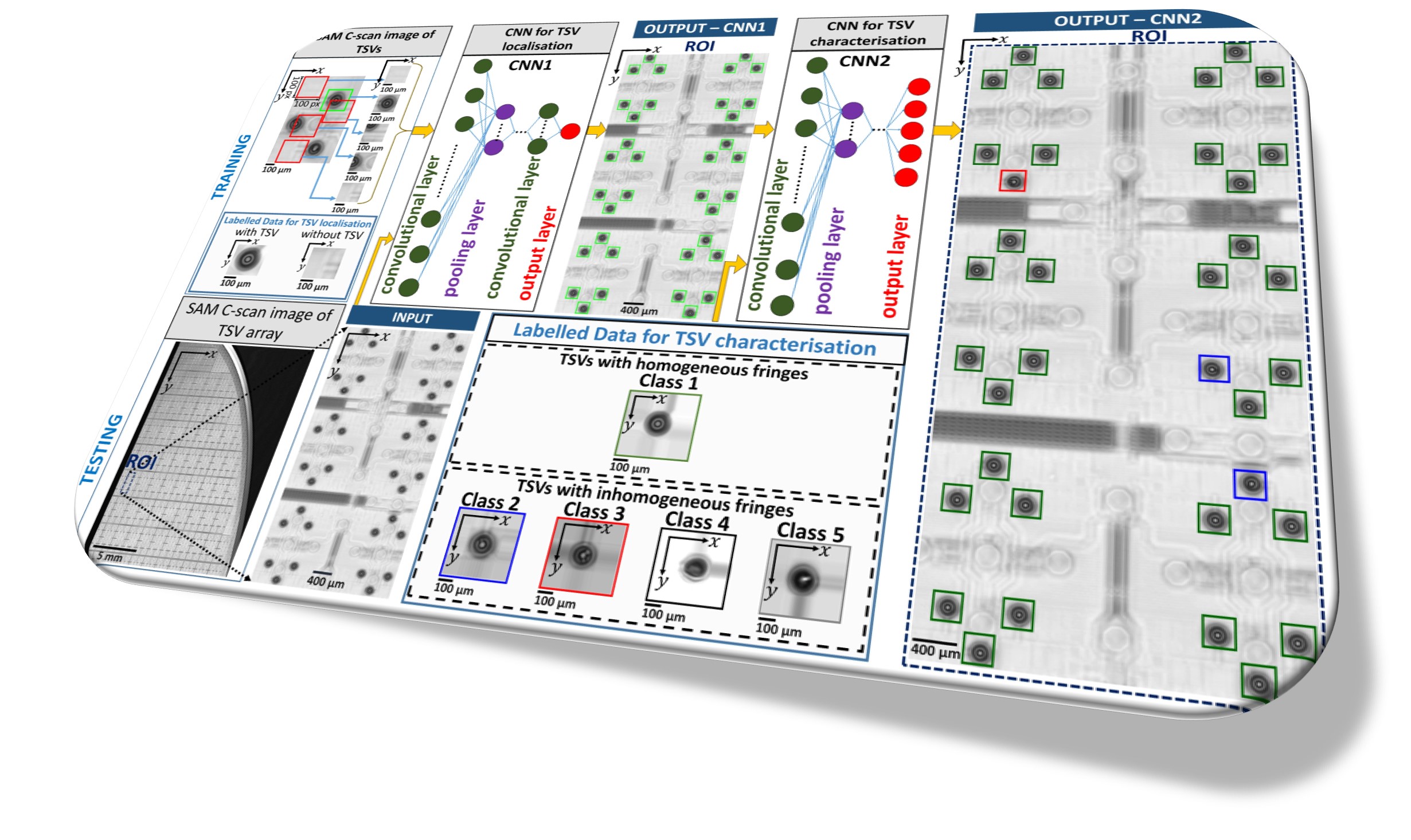
For modern non-destructive failure analysis, like in aerospace, rail-track inspection, civil engineering, automotive industry, power electronics, or microelectronics, etc. computational assisted imaging-based techniques are highly important.
In particular machine learning (ML) algorithms can provide here novel possibilities for efficient failure analysis of the generated complex data sets that previously relied mainly on human expertise. Within an industrial environment fully automated models are essential, which do not necessarily rely on specific training features and work in a reliable and robust manner.
In the field of microelectronics and power semiconductors decreasing structural sizes and increasing integration densities have led to the 3D-integration technology. It allows a vertical arrangement of different devices and offers clearly possibilities to continue the trend of miniaturization.
Within 3D integration, through silicon vias (TSVs) display a high-performance interconnection technology and offer vertical electron connection that can pass through a silicon wafer or die.
Modern failure inspection of TSVs demands cost- and time-efficient characterization of hundreds or even up to thousands of TSVs including the concomitant statistical information, the localization and status of the individual TSV covering the entire geometry with its bottom and sidewall as well as the classification of the TSV failure.
There are various defect types related to TSVs including voids resulting from electroplating, delaminations arising due to thermal expansion mismatch, cracks resulting from global stress in the die warpage and so on.
State of the art techniques show respective advantages as well as disadvantages that restrict their application for efficient TSV failure analysis. A non-destructive imaging technique with potential in this context displays scanning acoustic microscopy (SAM) capable to characterize time- and cost-efficiently large regions of interests as well as to produce sufficient statistical data output.
The main challenge of this method lies in the limited resolution and contrast as well as in the post-processing of the generated image data set, namely to extract efficiently knowledge about the location of the individual failure but also about the statistical distribution of the failures within the array including the type of the defect class. Therefore, it requires a careful manual inspection of the collected image data. In general, a manual inspection highly depends on the experience of the human user, is therefore subjective and in addition prone to error.

The Materials Center Forschung GmbH, ams-Osram and PVA TePla Analytical Systems developed within the FFG Project Proj. No. 872629 REFORM and partly within the COMET framework an End-to-End Convolutional Neural Network (E2E-CNN) enabling the fully automated failure localization and classification of TSV arrays. Therefore, a unique scanning acoustic microscopy (SAM) approach was conducted to gain the relevant image data of the TSVs and ensure the necessary resolution and contrast for the failure detection.
The fully automated E2E-CNN network, uses two sequentially linked CNN architectures, which assure an accuracy for the detection and classification of the TSVs of 100% and greater than 96%, respectively and is capable to classify thousands of TSVs.
Notably, the presented approach is not limited to SAM-based image data, but rather displays a general approach applicable to other imaging methods e.g. XRM, SEM, optical microscopy etc. .
A link to the manuscript can be found here: An end-to-end convolutional neural network for automated failure localisation and characterisation of 3D interconnects | Scientific Reports (nature.com)
Follow the Topic
-
Scientific Reports
An open access journal publishing original research from across all areas of the natural sciences, psychology, medicine and engineering.
Related Collections
With Collections, you can get published faster and increase your visibility.
Advances in neurodegenerative diseases
Publishing Model: Hybrid
Deadline: Jun 30, 2026
AI for clinical decision-making
Publishing Model: Open Access
Deadline: Jun 23, 2026



Please sign in or register for FREE
If you are a registered user on Research Communities by Springer Nature, please sign in