Foundry-compatible patterning of organic electronics
Published in Electrical & Electronic Engineering

High-performance thin-film transistors (TFT) are the core components of the backplane technology in the flat panel display industry, and are also an important part of improving the display effect of electronic equipment and reducing costs. At present, transistors based on silicon semiconductors are still the most widely used in commerce. However, with the development of flexible, large-area, high-resolution, and three-dimensional display technologies, the low mobility of amorphous silicon and the poor performance uniformity of brittle polysilicon limit their application in these fields.
Organic semiconductors have received extensive attention due to their good mechanical flexibility, mobility, diversity of raw materials, and roll-to-roll printing and manufacturing. After decades of development, organic transistors manufactured by the solution method are on the verge of large-scale industrialization. In the manufacturing process of pixelated films, the solution processability of polymer semiconductors becomes a disadvantage because the underlying film is susceptible to subsequent solvents. The impact of exposure. The patterning process compatible with the foundry must meet the following requirements, including high-throughput and high-resolution patterning, wide versatility, environmental processability, environmentally friendly solvents, and minimal device performance impact. However, the known methods can only meet very few of these requirements.

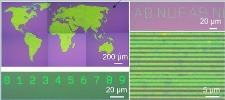
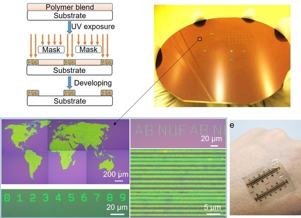
Figure 1: Large-area patterning of organic thin films by three-step photolithography and their ultrathin and ultraflexible devices.
We propose a vertical phase separation film mechanism for three-step lithography commercial semiconductor polymer films to achieve foundry compatibility with high-resolution patterning. The process involves a vertical phase separation mixture of cross-linked semiconducting polymers and ultraviolet light curable additives, and the use of environmentally friendly solvents can be used for photo-patterning in an air environment with a resolution of up to 0.5 microns in just three steps. Patterned semiconductor films can be integrated into thin-film transistors, which have excellent transfer characteristics, low off-current and high thermal (up to 175 °C) and chemical (soaked in chloroform for 24 hours) stability. In addition, these patterned organic structures can also be integrated on a 1.5 micron thick substrate to prepare highly mechanically flexible thin film transistors (resistant to 5,000 times @1 mm radius bending).
The research project lasted three and a half years from generating ideas to articles online, involving semiconductor devices, materials science, physics and chemistry and other disciplines. Dr. Wang said that the two major challenges are 1) the use of multiple characterization techniques including synchrotron radiation, X-ray photoelectron spectroscopy, and atomic force microscopy to study the experimental mechanism; 2) the preparation of ultra-thin and ultra-flexible organic transistor arrays.
For more information, please check out our article “ Foundry-compatible high-resolution patterning of vertically phase-separated semiconducting films for ultraflexible organic electronics”published in Nature Communications.
Follow the Topic
-
Nature Communications
An open access, multidisciplinary journal dedicated to publishing high-quality research in all areas of the biological, health, physical, chemical and Earth sciences.
Related Collections
With Collections, you can get published faster and increase your visibility.
Women's Health
Publishing Model: Hybrid
Deadline: Ongoing
Biosensing
Publishing Model: Hybrid
Deadline: Jun 30, 2026


Please sign in or register for FREE
If you are a registered user on Research Communities by Springer Nature, please sign in