Giant tunnel electroresistance through a Van der Waals junction by external ferroelectric polarization
Published in Materials, Physics, and Computational Sciences

Two-dimensional (2D) semiconductors with their unique layered van der Waals architecture, absence of interlayer binding constraints, and remarkable mechanical resilience have emerged as highly promising candidates for next-generation semiconductor technology. MoS2 stands out as one of the extensively investigated 2D semiconductors due to its exceptional properties, boasting well-defined bandgap, stability in ambient conditions, and relatively high charge carrier mobility. These unique attributes position MoS2 at the forefront of modern electronics and optoelectronics, encompassing memories and photodetectors based on field-effect transistors (FETs). However, most of advancements have focused on the development of n-type transistors while achieving programmable ambipolar operation within the same MoS2 FET remains an elusive goal. An approach to reversible ambipolar MoS2 FETs on the same chip without intrinsic/extrinsic doping or complex processing steps is highly desirable.
The expertise in our team:
It is a big ferroelectric team at key laboratory of polar materials and devices, Ministry of Education, East China Normal University including but not limited to Prof. Chu, an academician of Chinese Academy of Sciences, Prof. Duan who devotes to the first-principles calculations for ferroics and Prof. Tian who focuses on ferroelectric memory and neuromorphic computing devices. This ferroelectric team contributes to the formation of various innovative concepts that play important role in ferroelectric communities, including “ferroelectric control of magnetism” [Phys. Rev. Lett. 97, 047201 (2006)], “multi-ferroelectric tunneling junction” [Nano Lett. 9, 427 (2009)], “ferrovalley” [Nat. Commun. 7, 13612 (2016)] and “ferroelectric fin diode” [Nat. Commun. 15, 513 (2024)]. This team reported the first organic ferroelectric tunneling junction [Nat. Commun. 7, 11502 (2016)] and recently demonstrated that ferroelectric local electric field can be used for programable electrostatic doping in 2D semiconductors [Nat. Electron. 3, 43 (2020)]. This nonvolatile and reconfigurable electrostatic doping technique by ferroelectric domains was further successfully used for emerging in-memory sensing and computing applications [Nat. Mater. 22, 1499 (2023)].
Innovative results:
It is reasonable for us to utilize a ferroelectric modulation to solve above mentioned issues. Indeed, we have demonstrated its efficacy of the ferroelectric gate as a powerful tool for electrostatic modulation in previous works. On one hand, ferroelectric polarization generates intense electric field of GV/m around the interface, enabling substantial modulation of carrier concentration and band structure within the nearby semiconductor. On the other hand, ferroelectric hysteresis endows electronic devices with memory functionality that has found applications in neuromorphic devices.
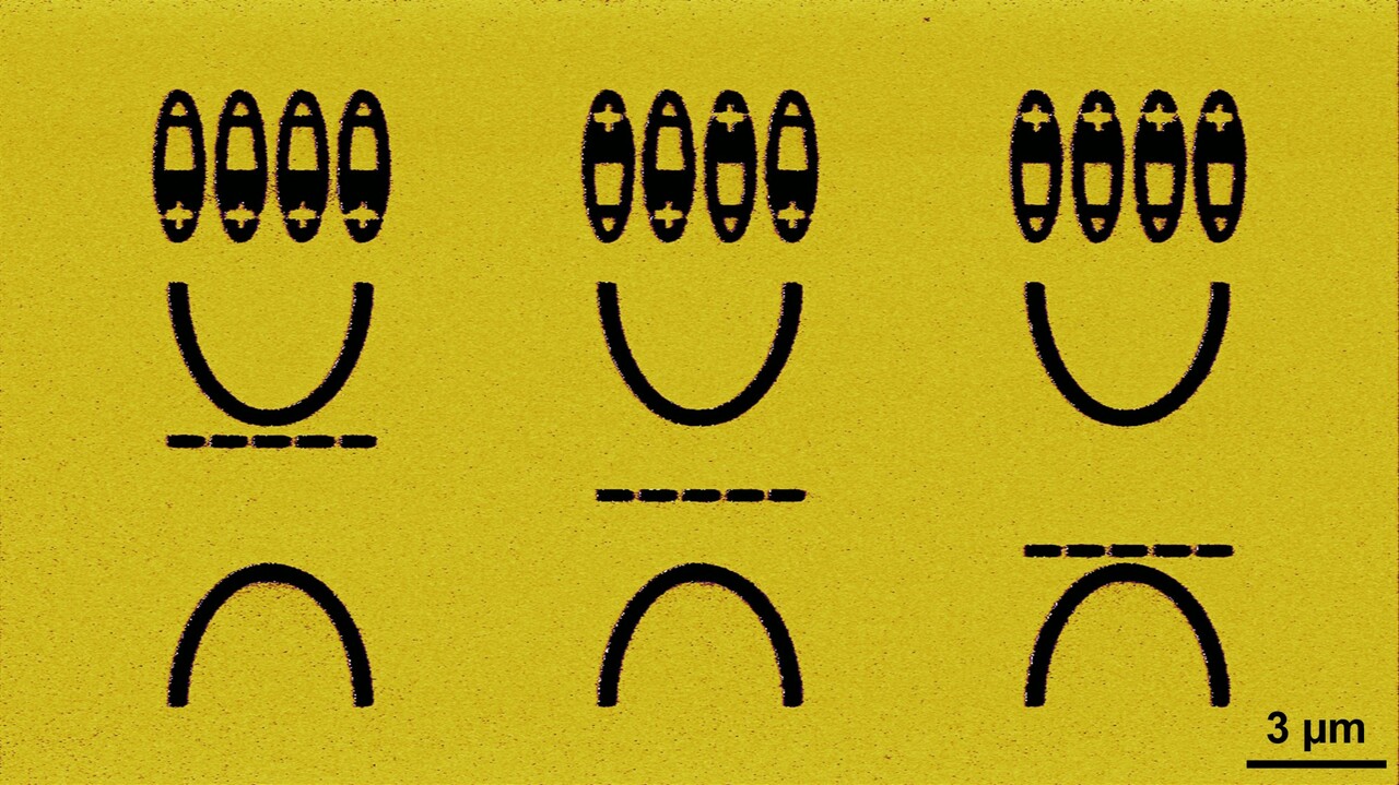
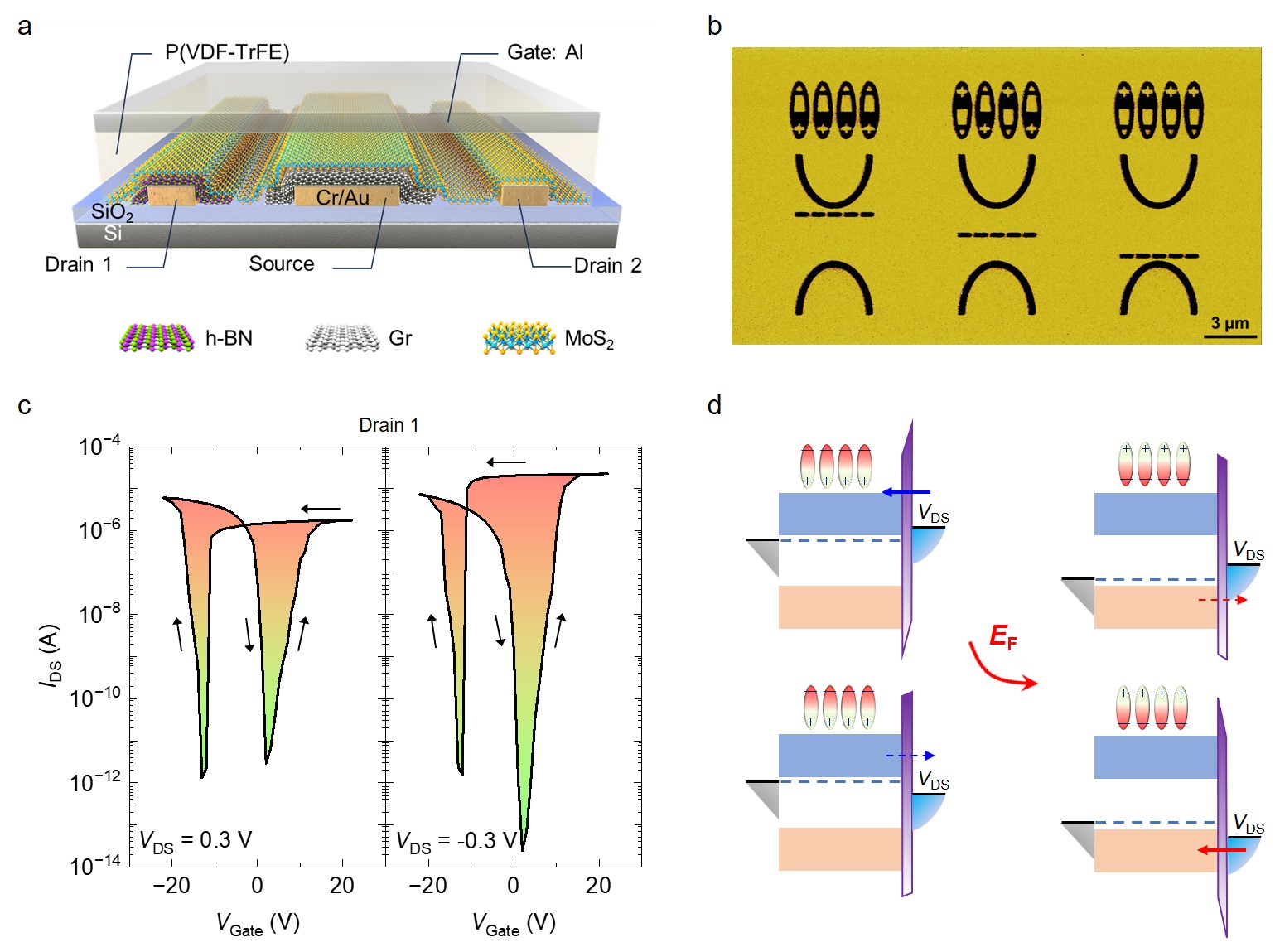
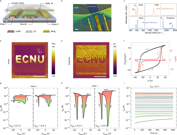
Herein, we propose a vertical tunneling ferroelectric FET (FeFET) in which the MoS2/h-BN/metal tunnel junction rather than a single semiconductor is designed as channel (Figure 1a). Mr. Liu and Dr. Feng fabricated and measured the conceptual device under the supervision of Prof. Zhu and Prof. Tian. As illuminated by a piezoelectric force microscope (PFM) phase image of ferroelectric polymers films in Figure 1b, the tunable Fermi level whose position ranges from bottom edge of conduction band to top edge of valence band depending on the ferroelectric domain orientation was observed, represented by the typical ambipolar behavior of the vertical tunneling MoS₂-FeFET (Figure 1c). Note that the change of Fermi level within the MoS2 electrode is read out through quantum tunneling currents across the atomic-thin h-BN layer (Figure 1d). Since the direct quantum tunneling strength is extremely sensitive to the barrier shape that is co-defined by MoS2 band alignments, the vertical tunneling MoS₂-FeFET exhibits a record high ON/OFF ratio of up to 109 (Figure 1c).

Figure 1 A vertical tunneling FeFET utilizing an asymmetric Van der Waals MoS2/h-BN/metal tunnel junction as channel. aSchematic of vertical tunneling MoS2-FeFET with ferroelectric P(VDF-TrFE) layer as ferroelectric gate and MoS2/h-BN/Au/Cr as channel. b A PFM phase image of ferroelectric polymers films in which the ferroelectric domains’ configuration illuminates the tunability of the Fermi level position by ferroelectric domains. c Transfer curves of the vertical tunneling MoS2-FeFET in a semilog plot, measured at VDS = ±0.3 V. d Schematic band alignments of the vertical tunneling MoS2-FeFET for downward (left panels) and upward (right panels) ferroelectric polarization states respectively.
The memory properties of the vertical tunneling MoS₂-FeFET are comprehensively explored. The vertical tunneling MoS₂-FeFET achieves a switching speed as fast as 500 ns. The energy consumption is calculated using the formula E=UIt, where U, I and t are the operating voltage amplitude, the leakage current and operating speed respectively. The gate leakage current of the vertical tunneling MoS2-FeFETs is at the picoampere level, pioneering energy consumption as low as 0.16 fJ per operation. The cycling tests show that the device still work well after 107 cycles. Furthermore, the vertical tunneling MoS₂-FeFET realizes 22 distinct conductance states with minor variation over a period of 103 s, indicating possible potential for robust multi-bit memory and neuromorphic computing applications.
It is worthy to compare the vertical tunneling FeFET with the Ferroelectric Tunneling Junction (FTJ) which takes advantage of direct quantum tunneling effect through the ferroelectric layer. In FTJ device, it typically requires the ferroelectric layer to be only a few nanometers. However, the coercive electric field in nano-scale ferroelectric thin films is significantly higher than that in bulky films, suffering from poor fatigue performance in FTJs (<106 cycles). Unlike FTJs, the ferroelectric layer in vertical tunneling FeFETs does not function as a tunneling layer but as a third control terminal, that is, the tunnel electroresistance through the below Van der Waals junction is achieved by modulating the Femi level of 2D semiconductor electrode by an external ferroelectric gate. This removes the thickness constraint imposed by quantum tunneling, effectively mitigating the fatigue issues associated with FTJs. The vertical tunneling MoS2-FeFET still work well after 107 cycles. Besides, the leakage currents in a vertical tunneling FeFET that pass through thick and insulative ferroelectric gate are much lower than the inevitable tunneling currents in FTJ, pioneering energy consumption as low as 0.16 fJ per operation.
Apart from these outstanding memory performances, this ingeniously devised structure also exhibits gate tunable operation states of output level, including positive-pass, OFF, negative-pass, and full-pass modes. Interestingly, a free-moving band alignment model is useful to elucidate the mechanisms underlying all these observed electrical properties. The large tunnel electroresistance through the Van der Waals junction by external ferroelectric polarization offers a platform as both precise Fermi level detection technique for physical research and new block of memory communities for storage applications.
This work is titled as “Giant tunnel electroresistance through a Van der Waals junction by external ferroelectric polarization” and published in the latest issue of Nature Communications (DOI: https://doi.org/10.1038/s41467-024-54114-3.
Follow the Topic
-
Nature Communications
An open access, multidisciplinary journal dedicated to publishing high-quality research in all areas of the biological, health, physical, chemical and Earth sciences.
Related Collections
With Collections, you can get published faster and increase your visibility.
Women's Health
Publishing Model: Hybrid
Deadline: Ongoing
Biosensing
Publishing Model: Hybrid
Deadline: Jun 30, 2026


Please sign in or register for FREE
If you are a registered user on Research Communities by Springer Nature, please sign in