Grain Boundaries Contribute to the Performance of Perovskite Solar Cells by Promoting Charge Separations
Published in Materials
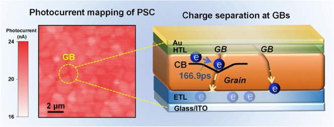

In a recent study published in Nano-Micro Letters, a collaboration led by Prof. Wenming Tian and Prof. Shengye Jin (Dalian Institute of Chemical Physics, CAS) and Prof. Yantao Shi (Dalian University of Technology) challenges the long-held belief that grain boundaries (GBs) in perovskite solar cells (PSCs) are detrimental to performance. Using operando, sub-micrometer imaging, the team reveals that GBs in high-efficiency devices can act as charge-separation “highways,” boosting photocurrent and aiding carrier extraction.
Why This Research Matters
- Direct evidence in operating devices: High-resolution confocal photoluminescence and photocurrent imaging show enhanced photocurrent at GBs with a clear anti-correlation to PL intensity—evidence of GB-driven charge separation.
- Built-in electric fields: Kelvin probe force microscopy detects strong local fields (102–103 V·cm⁻¹) at GBs, while transient absorption microscopy confirms ultrafast electron–hole separation (~167 ps) and a threefold longer lifetime of separated states at GBs (~14.5 ns) compared to grain interiors (~5.0 ns).
- Performance correlation: Devices with higher efficiencies (up to 22.45% PCE) exhibit greater GB-induced photocurrent enhancement (~5%) than lower-performing devices (~1.4%).
- Design insight: Rather than eliminating GBs, engineer them—passivate traps but preserve beneficial built-in fields to enhance carrier extraction.
Innovative Design and Mechanisms
- Operando correlative mapping: Custom-built imaging on thin ITO substrates achieves ~300 nm PL and ~500 nm photocurrent resolution in full device stacks, capturing real GB effects under realistic, bias-free conditions.
- Field-guided transport: GB-induced band bending channels electrons and repels holes, creating preferential carrier pathways and reducing recombination.
- Processing–function link: Adjusting annealing times modifies GB crystallinity and defect density, tuning the local electric field and net performance contribution.
Applications and Future Outlook
- Perovskite film optimization: Focus on GB engineering rather than removal to maximize their positive role in high-PCE devices.
- Module manufacturing: The operando imaging approach offers a powerful screening tool for scalable production.
- Cross-material relevance: The GB-field concept can extend to other polycrystalline optoelectronics such as CdTe, CIGS, and thin-film transistors.
By reframing grain boundaries from a problem to a design opportunity, this work provides a new direction for advancing perovskite photovoltaics toward higher efficiency and stability.
Editor of Nano-Micro Letters, which is an Open-Access, peer-reviewed journal reported papers that have at least one dimension ranging from a few sub-nanometers to a few hundreds of micrometers. The journal is published by Springer Nature and indexed by SCI, EI, SCOPUS, Pubmed, etc. The 2025 JCR Impact Factor is 38.5. The 2025 CiteScore is 58.9.
Follow the Topic
-
Nano-Micro Letters
Nano-Micro Letters is a peer-reviewed, international, interdisciplinary and open-access journal that focus on science, experiments, engineering, technologies and applications of nano- or microscale structure and system in physics, chemistry, biology, material science, and pharmacy.


Please sign in or register for FREE
If you are a registered user on Research Communities by Springer Nature, please sign in