Helium spin-echo spectroscopy allows scientists to make 2D materials with tailored holes
Published in Chemistry

Helium scattering is one of the most sensitive analytical techniques to study the surfaces of materials and the reactions that take place on those. Helium Spin-Echo (HeSE) has been successfully applied to reveal, with unprecedented detail and time-resolution, the fast motion of atoms and molecules on crystal surfaces, including quantum motion of protons and ballistic diffusion of molecules[1,2,3,4,5].
Evolution of ordered nanoporous phases during chemical vapour deposition
In a study recently published in Nanoscale Horizons, Dr Anton Tamtögl (Graz University of Technology) and his group, together with Dr Nadav Avidor who supervised the measurements, employed the HeSE technique to monitor the growth of one of the most promising 2D materials, hexagonal boron nitride (h-BN)[6]. h-BN has a 2D honeycomb crystal structure identical to that of the most famous 2D material, graphene, but with alternating boron and nitrogen atoms replacing the carbon atoms of the hexagon. h-BN finds applications in several microelectronic and nanotechnology applications, including photonic and power devices, fuel cells and as dielectrics for field-effect transistors[7].

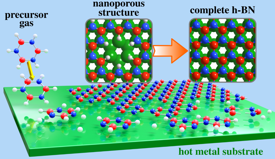
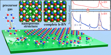
As illustrated in the figure, atomically thin 2D materials are nowadays frequently grown by exposing a hot metal surface to a specific gas, with the gas consequently decomposing on the hot metal substrate and forming the desired 2D material. Naturally, there are several intermediate steps involved, before the 2D material is completed. However, the evolution of this process is seldomly studied in experiments, since it is extremely difficult to directly monitor the growth process (due to high temperatures and the fast conversion).
The measurements show that, before h-BN was formed, other 2D surface structures could be isolated. Quantum mechanical calculations performed by the Group of Dr Marco Sacchi at the University of Surrey have allowed the scientists to understand that these ordered structures are made by regularly spaced holes (so-called nanopores) of h-BN. This is the first time that these open structures have been identified and their role during the growth of h-BN is observed[6].
“We were amazed to see that, instead of the expected diffraction pattern of hexagonal boron nitride, we recorded a very different one, which we then assigned to a novel phase [a 3 × 3] of h-BN” declares Dr Tamtögl, who led the experimental work.”
“Finding a new phase for such a well-known and technologically important 2D material is like discovering a completely new species of butterfly in your own garden” adds Dr Ruckhofer, who performed the experiments as part of his PhD research. “We wanted to be sure of our findings before publishing this discovery and we needed help from theory to confirm that what we saw was possible”.
The Group of Dr Marco Sacchi, at the University of Surrey, took on the challenge and performed quantum chemical calculations using the ARCHER2 national facility. “We investigated several theoretically possible open network phases of h-BN and we found one that was clearly preferred and that corresponded to the same 3 × 3 pattern as observed in the experiments.”
Outlook for other 2D materials and relevance for nanotechnology
The scientists are optimistic about the impact and future of this research. Dr Avidor, who supported the project as the Facility Development Scientist of the Cambridge Atom Scattering Facility, explains that “the exclusive surface sensitivity of helium scattering allowed us to see how molecules re-form into atomically thin networks, which in-turn convert to 2D hexagonal boron nitride”. Dr Sacchi adds, “We proved that the combination of experiments and quantum chemical calculations can provide new and important insight into the growth of 2D materials”, and continues: “And we are already planning to employ our method for studying the growth of other 2D materials”.
Dr Tamtögl concludes. “The nanoporous phases discovered during our research are not of purely academic interest, but they could find applications as sensor materials, nanoreactors, and membranes. It illustrates that fundamental physics and chemistry are still very much relevant for nanotechnology.”
- M. Sacchi & A. Tamtögl, Adv. Phys. X 10.1080/23746149.2022.2134051 (2022).
- A. Tamtögl et al., Motion of water monomers reveals a kinetic barrier to ice nucleation on graphene. Nat. Commun. 12, 3120 (2021).
- A. Tamtögl et al., Nanoscopic diffusion of water on a topological insulator. Nat. Commun. 11, 278 (2020).
- A. Tamtögl, Schnelle Bewegungen auf Oberflächen messen. Nachr. Chem., 68, 65, (2020)
- E. Bahn et al., Structure and dynamics investigations of a partially hydrogenated graphene/Ni(111) surface. Carbon 114, 504 (2017).
- A. Ruckhofer et al., Evolution of ordered nanoporous phases during h-BN growth: controlling the route from gas-phase precursor to 2D material by in situ monitoring. Nanoscale Horiz. 10.1039/D2NH00353H (2022).
- K.Y. Ma et al., Epitaxial single-crystal hexagonal boron nitride multilayers on Ni (111). Nature 606, 88 (2022).


Please sign in or register for FREE
If you are a registered user on Research Communities by Springer Nature, please sign in