High-performance, power-efficient three-dimensional system-in-package designs with universal chiplet interconnect express
Published in Electrical & Electronic Engineering
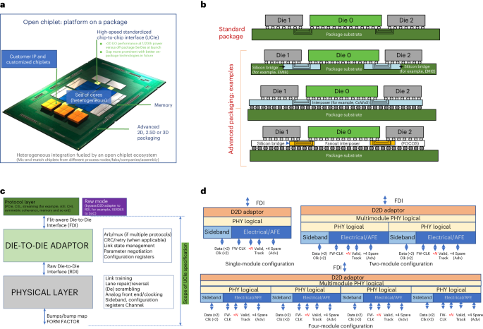
On-package integration of chips in commercial systems dates back multiple decades. Intel’s Paxville processor was the first dual-core Xeon launched in 1998 more than 25 years ago. Since CPUs were multi-drop front-side-bus (FSB) based, two single core chips were connected using their FSB interface in the package which was then ported out to connect to other components on the motherboard. This provided the compute density without requiring redesign of the chip. Multi-core Xeons have since been monolithic designs for lower cost and better power-performance. However, with the slow-down in Moore’s law, the high cost in the advanced process nodes, the yield challenges with larger dies in the advanced process nodes, and the exponential compute and memory bandwidth demand, we see the deployment of multiple chiplets in mainstream commercial offerings across the entire spectrum of compute. These include offerings from multiple companies in the hand-held, mobile, server CPUs, GP-GPUs, on-package memory, etc., connected using proprietary technologies, both planar as well as three-dimensional (3D), using standard as well as advanced packaging techniques.
Our experience with on-package interconnects extends over a decade with Intel’s multiple product offerings. The recent Intel’s 4th Gen Intel® Xeon® Scalable CPU relied on a challenging die-to-die interconnect using Intel’s Embedded Multi-die Interconnect Bridge (EMIB). Up to 4 CPU chips were connected to deliver similar performance as a single large die with the same core count as 4 dies. Xeon CPUs require high bandwidth density with very stringent power and latency requirements. This caused us to rethink the whole interconnect architecture and we delivered the key performance metrics with very high quality. The evolution of the technology continued. After three generations, we felt it was appropriate to donate the technology to the broader industry as a specification that the entire ecosystem can evolve. The Universal Chiplet Interconnect Express (UCIe) consortium was born with Intel donating the UCIe 1.0 specification to enable a plug-and-play ecosystem. UCIe 1.0 supported both standard (2D) and advanced packaging in planar (2.5D), with well-defined internal interfaces to support a range of protocols (e.g., PCI-Express and Compute Express Link, CXL, which are widely deployed at the board level across all types of systems to interconnect components), supporting a range of interoperable frequencies from 4GT/s to 32GT/s, with aggressive latency and power consumption expectations. UCIe is modeled after Intel’s successful launch of industry standards such as Peripheral Component Interconnect Express (PCIe), Compute Express Link (CXL), Universal Serial Bus (USB), etc. The goal is to mix-and-match chiplets from different sources that a designer can package together, that will unleash innovations at a package level, similar to what we have been able to do at a board level with PCIe, CXL, and USB.
One of the natural questions that arises is how does performance scale with UCIe going forward? Unlike board-level interconnects such as PCIe, which is circuit area limited, UCIe is bump area limited, which presents tremendous opportunities. The trend in on-package interconnects, especially with advanced 3D interconnect technologies such as hybrid-bonding, is reduced bump pitches going down from 25u to 1u and below. Bump pitch is the minimum distance between two connectivity points at the chiplet level that will be used to connect to its neighboring chiplet. When bump pitch reduces, the available area under the bump goes down as a square of the bump pitch reduction, but the number of wires in a given area goes up as a square. Thus, if the bump pitch goes down from 45u (current technology volume sweet-spot with advanced packaging covered by UCIe 1.0) to 1u (the future trend), we get 2,025 times as many wires in the same area. With the number of wires growing exponentially, our strategy is to reduce power by reducing the frequency. This research paper delves into the architectural choices that should be made as the industry and UCIe prepares to move towards 3D integration of chiplets with reduced bump pitches. Our proposed frequency reduction results in simpler circuits, making them fit within the bump area. We still get the higher bandwidth due to number of wires increasing exponentially. For example, our proposal is to run the wires at 1GT/s at 1u in the future while currently we run UCIe 1.0 at 45u at a maximum frequency of 32GT/s. Even with a 32x reduction in frequency, we get about 64x improvement in bandwidth density, but the power reduction is 25x (from 0.25 pJ/b to 0.01pJ/b). More importantly, with 3D integration, we don’t consume any shoreline of the chiplet since we don’t have to route signals to the edge of the die – the connections can be across the chiplets vertically in-place, not consuming any extra area for routing of signals inside the chiplet. Thus, we get the entire surface area (as opposed to the edge) with 3D integration vs planar interconnects. We compare the performance of the UCIe-3D chiplets using our approach with an imaginary, ideal, large monolithic die that has no area or yield constraints. Our results demonstrate something very counter-intuitive: small chiplets connected using our proposed UCIe-3D interconnect outperform the ideal monolithic chip! The rationale is that with 3D, both maximum and average distances reduce. Lower distance results in less latency to transfer bits and hence consume less power. This results in lower power and higher performance.
The vision we put forth in this article is a system on a package with several UCIe-3D chiplet stacks that are connected using existing UCIe-2.5D and UCIe-2D planar interconnects. We envision off-package connectivity through co-packaged optics and traditional electrical signaling using on-board traces and/or electrical cables. This level of integration is much more than what the industry does today. Today’s chiplet integration on-package will look like small towns where density is higher than monolithic chips of a decade back, which were like villages. Our vision with UCIe-3D is one of a metropolis with skyscrapers which offers very high density. High density of compute and memory elements closely packaged together means less distance for bits to travel – this results in less power while delivering superior performance. There will be several challenges such as power delivery, cooling, testability, debug, yield, and field repair that we need to address to make this vision a reality. However, any major transition that delivers exponential benefits such as our proposed dense 3D chiplet vision is always associated with seemingly insurmountable challenges that the researchers and practitioners eventually solve. With the combined might of an open standard and ecosystem like UCIe, these challenges will be solved, like we have done with PCI-Express over two decades. We invite the broad community to get involved, innovate, and solve these challenges that will make the next-generation computing platforms more powerful and greener.
Follow the Topic
-
Nature Electronics
This journal publishes both fundamental and applied research across all areas of electronics, from the study of novel phenomena and devices, to the design, construction and wider application of electronic circuits.


Please sign in or register for FREE
If you are a registered user on Research Communities by Springer Nature, please sign in