How to design a photogating or photoconductive effect in phototransistors
Published in Electrical & Electronic Engineering


2D Transition Metal Dichalcogenides (TMDCs) have been actively studied in recent times due to their interesting electronic and optoelectronic properties. In particular for photodetection applications, TMDCs display direct to in-direct band gap transitions and broadband light detection based on layer tuning. Although great effort has been made to design high responsivity photodetectors by discovering new materials, different device structures, material doping, and combining different materials to create heterostructures, an understanding of how to intrinsically enhance the light sensitivity has not yet been discussed. Obtaining a better understanding of modifying the photocurrent generation process can help to provide a tool to design photodetectors for specific types of applications.
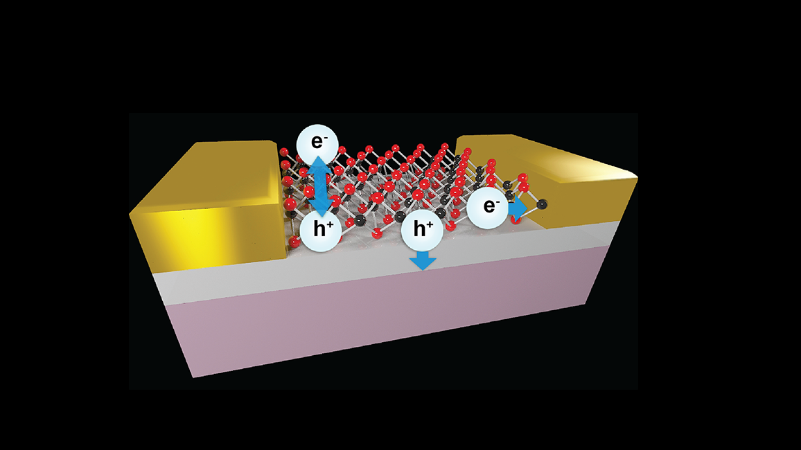
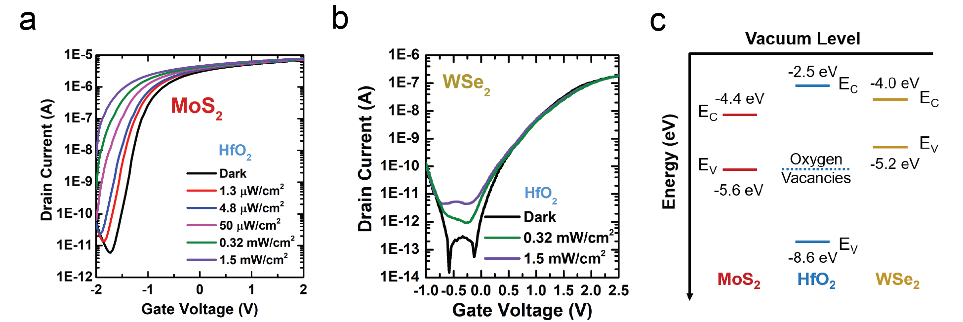
In this study, we investigated how to design a dominating photogating or photoconductive effect with TMDC-based phototransistors. The photoconductive effect can provide fast light switching speeds due to collection of photogenerated carriers and the photogating effect can provide high light sensitivity due to photocarrier charge trapping. Although many works have reported photogating behavior for TMDCs, this behavior as a dominating photocurrent generation mechanism is observed in the accumulation mode only. Here, we explored how the dielectric layer properties can directly influence the photocurrent generation process. High-k metal oxides such as hafnium oxide (HfO2) are well known charge trapping materials which are used in some memory applications. We found that the intrinsic oxygen vacancy defects located in the mid band gap region of HfO2 offers trap energy level alignment with the valence band edge of MoS2. As a result, the photogenerated holes tunnel into the HfO2 dielectric layer to occupy these defect levels enabling a strong photogating behavior as seen in the figure 1(a) below. By providing a trap energy level misalignment, a strong photoconductive effect can be observed with the WSe2 device in figure 1(b) using the same HfO2 dielectric. The band energy diagram of MoS2, WSe2, and HfO2 in figure 1 (c) illustrates the valence band alignment with these oxygen vacancies.
As a result of creating a dominant photogating photocurrent generation, we were able to achieve a high peak responsivity of 1x10⁶ A/W for intrinsic MoS2 and photocurrents as high as 2 μA. Our work shows how tuning the valence band edge alignment with known intrinsic dielectric defects can enable a strong photogating or photoconductive effect for the photocurrent generation process in phototransistors.
If you are interested in learning more about this study, please check out our article published in Communications Materials titled:
“High Responsivity in MoS2 Phototransistors Based on Charge Trapping HfO2 Dielectrics”:
https://www.nature.com/articles/s43246-020-00103-0
Co-authors:
Dr. Takashi Tsuchiya, Dr. Kasidit Toprasertpong, Dr. Kazuya Terabe, Prof. Shinichi Takagi, and Prof. Mitsuru Takenaka
Follow the Topic
-
Communications Materials

A selective open access journal from Nature Portfolio publishing high-quality research, reviews and commentary in all areas of materials science.
Related Collections
With Collections, you can get published faster and increase your visibility.
Advanced characterizations of high-entropy materials
Publishing Model: Open Access
Deadline: Mar 31, 2026
Multifunctional hydrogels
Publishing Model: Open Access
Deadline: Feb 28, 2026


Please sign in or register for FREE
If you are a registered user on Research Communities by Springer Nature, please sign in