Implementation of ultra-scaled capacitor-less DRAM cells using III-V materials
Published in Electrical & Electronic Engineering
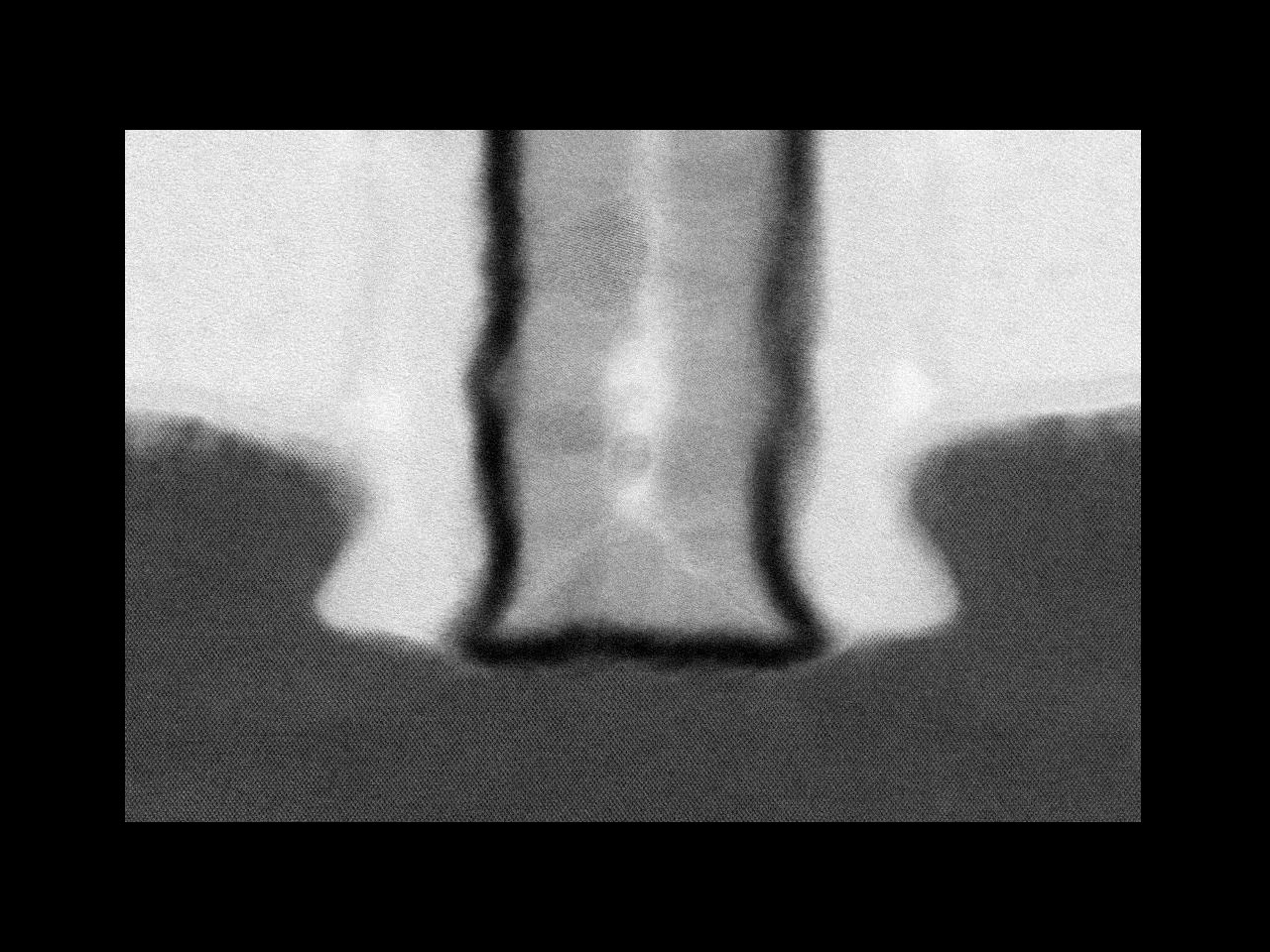
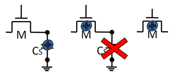
In 1966, Dr. Robert Dennard devised the idea of combining a transistor and a capacitor (1T+1C) to obtain a single-bit storing circuit element: The transistor controls the access to the capacitor which is responsible for 'storing' the information as charge. One year later, Dr. Dennard and IBM filled a patent application for the single-transistor dynamic random access memory (DRAM). From this very moment, the 1T+1C DRAM became gradually used in digital electronics where high-density and low-cost memories were necessary. Nowadays, DRAM chips can be easily found as the 'main memory' in all modern computers implementing the Von Neumann’s architecture.
Although the main concept and its principles of operation have remained essentially unchanged, the original bit cell has suffered a tremendous downscaling. This cell size reduction implies important structural modifications where the fabrication of the capacitor always represents the biggest challenge due to its large size and the use of exotic insulating materials. Today, in order to overcome this problem and further reduce the cost per cell, Dennard’s DRAM cell can be simplified by removing the capacitor and storing the charge within the transistor itself. This alternative, known as capacitor-less DRAM cells (or 1T-DRAM), has been extensively studied in silicon in the last 20 years. However, few studies have been carried out in other materials so far.
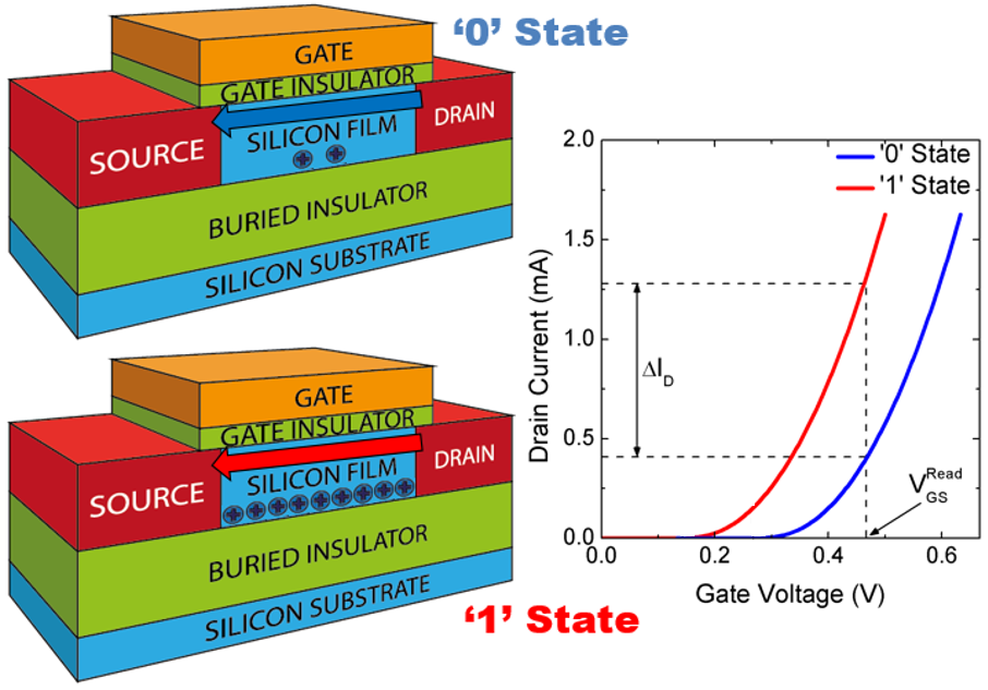
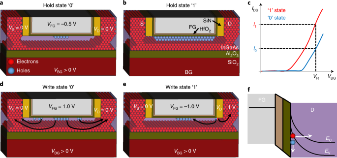
The 1T-DRAM operation is based on introducing charge inside the body of the transistor and modulate its inner electrostatic conditions so that different output current levels can be achieved. Each of these current levels is then associated with a logic state, '1' or '0', providing the memory operation.
Previous 1T-DRAM results with III-V compounds were based on TCAD simulations. They confirmed that the memory operation was feasible but no experimental result was yet available in any full III-V cell. Within the H2020 European REMINDER project (687931), focused on the implementation of innovative low-power IoT (Internet of Things) embedded memories, we wondered if these III-V alternative compounds could be experimentally implemented and operate as well as capacitor-less cells. Thanks to the collaboration of IBM Research Zürich in Switzerland, indium gallium arsenide (InGaAs) transistors were fabricated and electrically characterized later at the University of Granada in Spain. The obtained experimental results validated the dynamic capacitor-less memory operation: Two different current levels (high and low) associated with each logic memory states ('1' and '0', respectively). The most surprising fact was to find the memory operation in ultra-scaled cells down to 14 nm gate length without a dedicated and time-consuming optimization fabrication process.
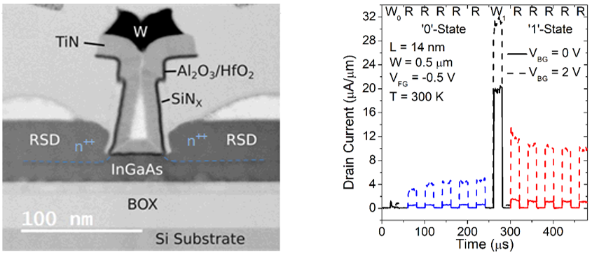
From the performance point-of-view, these novels III-V cells do not still reach the silicon capabilities in terms of retention and current margin. However, looking into the future, the optimization avenues are countless: From employing other III-V compounds or heterostructures to completely new cell architectures. Besides, the reported III-V 1T-DRAM cells potentially allow for reduced power consumption with respect to silicon thanks to the lower required biasing conditions and present the shortest gate length ever demonstrated in a 1T-DRAM. We expect this work to encourage the research of innovative 1T-DRAM cells, especially those based on alternative materials for future applications.
If you want to see more, please find our paper recently published in Nature Electronics, 'Capacitor-less dynamic random access memory based on a III–V transistor with a gate length of 14 nm': https://www.nature.com/articles/s41928-019-0282-6
Follow the Topic
-
Nature Electronics

This journal publishes both fundamental and applied research across all areas of electronics, from the study of novel phenomena and devices, to the design, construction and wider application of electronic circuits.


Please sign in or register for FREE
If you are a registered user on Research Communities by Springer Nature, please sign in