Mixed-Dimensional Nanowires/Nanosheet Heterojunction of GaSb/Bi2O2Se for Self-Powered Near-Infrared Photodetection and Photocommunication
Published in Materials

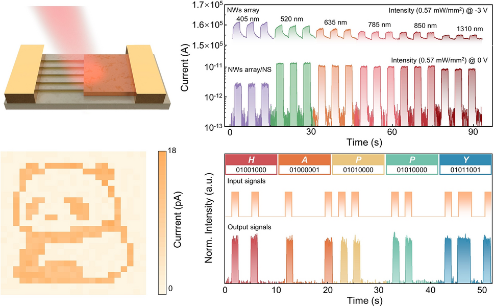
In the rapidly advancing field of optoelectronics, self-powered near-infrared (NIR) photodetectors are gaining attention for applications in imaging, environmental monitoring, and optical communication. Recently, a research team from Shandong University led by Professor Zai-xing Yang has made a significant leap forward by constructing a novel mixed-dimensional heterojunction between GaSb nanowires (NWs) and Bi2O2Se nanosheets (NSs). This breakthrough device demonstrates ultralow dark current, ultrafast response, and multifunctional capabilities — all without an external power supply.
Why This Research Matters
- Record-Low Dark Current: The GaSb/Bi2O2Se NW/NS and NW array/NS devices achieve ultralow dark currents of 0.07 pA and 0.08 pA, respectively, enabling exceptionally clean signal detection.
- Ultrafast Response: Response times of < 2 ms (single NW/NS) and 6/4 ms (NW array/NS) outperform most comparable systems, crucial for high-speed data processing.
- Broadband Sensitivity: Effective photodetection from visible to 1310 nm wavelengths makes these devices versatile for diverse NIR applications.
- Integrated Functionality: Beyond detection, the devices successfully demonstrated self-powered imaging and optical data transmission.
Innovative Design and Mechanisms
- Mixed-Dimensional Type-II Heterojunction: Combining 1D GaSb NWs and 2D Bi2O2Se NSs yields a built-in electric field (~140 meV) that promotes rapid, bias-free separation of photo-generated carriers.
- Array Architecture for Enhanced Performance: Ordered NW arrays, fabricated via contact printing, provide larger active areas, stronger photocurrents, and improved Ilight/Idark ratios.
- Interface Characterization: Advanced tools such as Kelvin probe force microscopy (KPFM), XRD, and AFM confirm precise band alignment and high-quality heterointerfaces.
Applications and Future Outlook
- Imaging: The team demonstrated single-pixel imaging of a “panda” highlighting potential for compact NIR cameras.
- Photocommunication: Successful ASCII code transmission (“HAPPY”) proves feasibility for secure, high-speed optical links.
- Next Steps: Scaling up fabrication, integrating with flexible substrates, and exploring other material pairings could open new pathways for wearable sensors, IoT devices, and space-borne imaging systems.
Stay tuned for more exciting developments from Prof. Yang’s group as they continue redefining the boundaries of self-powered optoelectronics and NIR photodetection technology.
Editor of Nano-Micro Letters, which is an Open-Access, peer-reviewed journal reported papers that have at least one dimension ranging from a few sub-nanometers to a few hundreds of micrometers. The journal is published by Springer Nature and indexed by SCI, EI, SCOPUS, Pubmed, etc. The 2025 JCR Impact Factor is 38.5. The 2025 CiteScore is 58.9.
Follow the Topic
-
Nano-Micro Letters
Nano-Micro Letters is a peer-reviewed, international, interdisciplinary and open-access journal that focus on science, experiments, engineering, technologies and applications of nano- or microscale structure and system in physics, chemistry, biology, material science, and pharmacy.


Please sign in or register for FREE
If you are a registered user on Research Communities by Springer Nature, please sign in