Modeling contacts to two-dimensional materials: importance of image forces and dielectric environment
Published in Electrical & Electronic Engineering

Transistors have been an integral part of modern electronic devices, and their performance is dependent on the choice of materials used in their construction. While Silicon has been the preferred material for transistor channels for many years, the emergence of two-dimensional (2D) materials, particularly transition metal dichalcogenides (TMDs), has opened exciting new possibilities for future electronic devices.
What makes these 2D materials so intriguing is their incredibly small thickness and unique electronic properties. These properties make them attractive candidates to make electronic devices that can deliver a large current, but there's a catch. TMDs are plagued by high contact resistance.
Contact resistance is the resistance encountered by current flow when it passes from one material to another at their interface. When a metal and 2D TMD comes in contact, a potential energy barrier is created at the junction due to the difference in their electronic properties. This barrier, known as the Schottky barrier, acts like a wall and can hinder the flow of electrons between the two materials, resulting in contact resistance. The higher the Schottky barrier, the worse is the contact resistance. The higher the contact resistance, the more difficult it is for electric current to pass through the interface, leading to reduced device performance. In short, contact resistance can be a significant challenge in designing and optimizing electronic devices due to the high Schottky barrier at the junction created by the contact metal to the 2D TMDs.
To tackle this problem, researchers have turned to theoretical studies using first principles density-functional theory (DFT) quantum transport calculations. These are tools to gain a deeper understanding of how the contact metal and semiconductor interact at the atomic scale and how that affects the Schottky barrier height and carrier injection process. However, computational challenges such as the need to simulate wide depletion regions, i.e., areas without charge carriers, requiring larger computational domains, increase the cost of DFT simulations and limit their applicability.
Moreover, a crucial phenomenon in metal-semiconductor contacts, known as image-force barrier lowering (IFBL), cannot be described by DFT and still remains to be explored in 2D contacts. When a metal electrode meets a semiconductor, image charges build up as carriers approach the interface, and the force between the injected carrier and its image lowers the barrier. This effect is always present in metal-semiconductor contacts and cannot be ignored whenever one tries to calculate contact resistance.
We were curious to see whether the choice of the dielectric environment would affect contact resistance in 2D materials. To do this we examined a contact geometry where the metal meets the 2D material at its edge, as shown in Fig. 1.
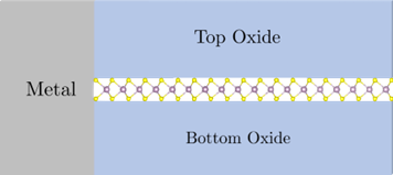
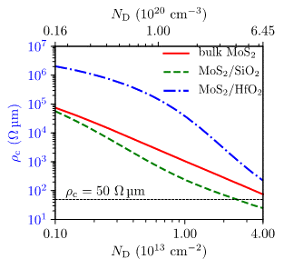
Through our research, we made an interesting discovery about the role of the dielectric environment surrounding the 2D channel in determining contact resistance. This factor distinguishes 2D geometries from bulk contacts, and we found that it plays a critical role in determining contact resistance in two ways: through depletion width and IFBL. Our findings showed that using insulators with high dielectric permittivity results in a larger depletion width, which in turn worsens the contact resistance. One interesting observation in our study is that with a low dielectric permittivity insulator such as SiO2, one can achieve a contact resistance in monolayer MoS2 that is lower than its bulk counterpart as demonstrated in Fig. 2. Additionally, we found that to achieve a contact resistance as low as 50Ω·μm, it is necessary to surround monolayer n-MoS2 (and monolayer p-WSe2) edge contacts with a low dielectric permittivity insulator and also dope them higher than 1×1013 cm−2 with work functions <5.1 eV (>4.6 eV). We also compared the effect of the coupling strength between the metal and semiconductor against that of the dielectric environment and found that a low dielectric permittivity insulator has a more significant impact on improving contact resistance than increasing the bond strength.
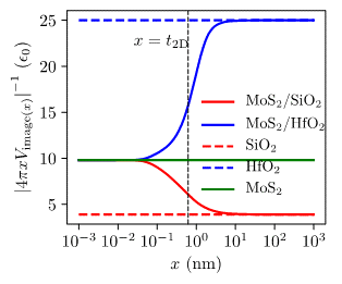
The theory of IFBL for bulk contacts has been well-established in textbooks through decades of research. However, it has not been explored much in the context of 2D contacts. To investigate how the dielectric environment affects IFBL (and ultimately, contact resistance) in 2D materials, we derived a new formula for IFBL and compared it with the conventional formula used for bulk contacts. We discovered that the conventional formula does not accurately predict the barrier lowering at various doping concentrations in 2D material contacts. At larger depletion widths, the barrier lowering is controlled by the surrounding dielectric permittivity, but that changes when one moves closer to the interface as seen in Fig. 3. Our study revealed that using a low dielectric permittivity insulator around the 2D channel results in more significant barrier lowering, which can lead to a 40 times improvement in contact resistance in metal-monolayer MoS2 edge-contact.
In conclusion, our research has shown that by understanding the impact of the dielectric environment and IFBL on contact resistance, researchers can develop new strategies to improve the performance of 2D materials in practical device applications. For more details on the implementation of the theoretical model and the results, check out our paper “The importance of the Image Forces and Dielectric Environment in Modeling Contacts to Two-dimensional Materials” https://www.nature.com/articles/s41699-023-00372-6
Follow the Topic
-
npj 2D Materials and Applications
This journal publishes papers on the fundamental behavior, synthesis, properties and applications of existing and emerging 2D materials.
Related Collections
With Collections, you can get published faster and increase your visibility.
Functionalization and Reactivity of 2D Materials
Publishing Model: Open Access
Deadline: Oct 06, 2026
2D Materials for Integrated Electronics
Publishing Model: Open Access
Deadline: Jul 18, 2026







Please sign in or register for FREE
If you are a registered user on Research Communities by Springer Nature, please sign in