One-dimensional vdW Tellurium Atomic Chains Encapsulated in Nanotubes: Towards the World’s Smallest Nanowire FETs
Published in Electrical & Electronic Engineering

With the fast development of large-scale integrated circuits, transistors have been built as small as a few nanometers in lab settings over the past few years. One way to shrink field-effect transistors (FET), the kind found in most electronic devices, is to build the gates that surround semiconducting nanowires, which puts forward an urgent requirement to exploit novel semiconducting materials much thinner than silicon.
As an attractive p-type elemental semiconductor, tellurium (Te) possesses a high electron and hole mobility of around 1000 cm2/Vs at room temperature. It has a unique DNA-like structure, in which atoms are strongly bonded with two nearest neighbors into helical chains along the [0001] direction, and the helical chains are stacked to form the Te crystal through weak van der Waals (vdW) interaction. This unique one-dimensional vdW crystal structure enables Te crystals to be isolated down to few atomic chains limit without breaking the crystalline integrity. However, the sensitivity of Te atomic chains in the ambient environment causes immense hardship to study the physical properties of 1D free-standing Te atomic chains. In order to stabilize 1D Te nanowire, carbon nanotubes (CNTs) was taken as templates during growth process. By carefully selecting the inner diameter of CNTs, controlling growth of ultra-narrow Te NWs with few-number of atomic chains can be realized (Fig. 1a-1e). This vdW-bonded 1D Te nanowires with single-atomic chain or few-atomic chains provides a potential scaling solution for FET applications.
The key issue with using CNTs is that their semiconducting or metallic nature will interfere with the electrical measurement of the filled materials. In contrast, electrically insulating BNNTs can provide an ideal protecting layer for such materials. Due to the excellent transport properties of Te and high thermal conductivity of BNNTs, the current-carrying capacity of BNNT-shielded Te NWs exceeds that of most semiconductor nanowires, reaching up to 1.5×10⁸ A/cm2. More importantly, both p-type and n-type Te FETs with few atomic chains as channels were successfully demonstrated by the shielding of BNNT combined with Al2O3 capping. The Te-BNNT FETs can smoothly functionalize even with the Te NW diameter scaled down to 2 nm (Fig.1f-1i).
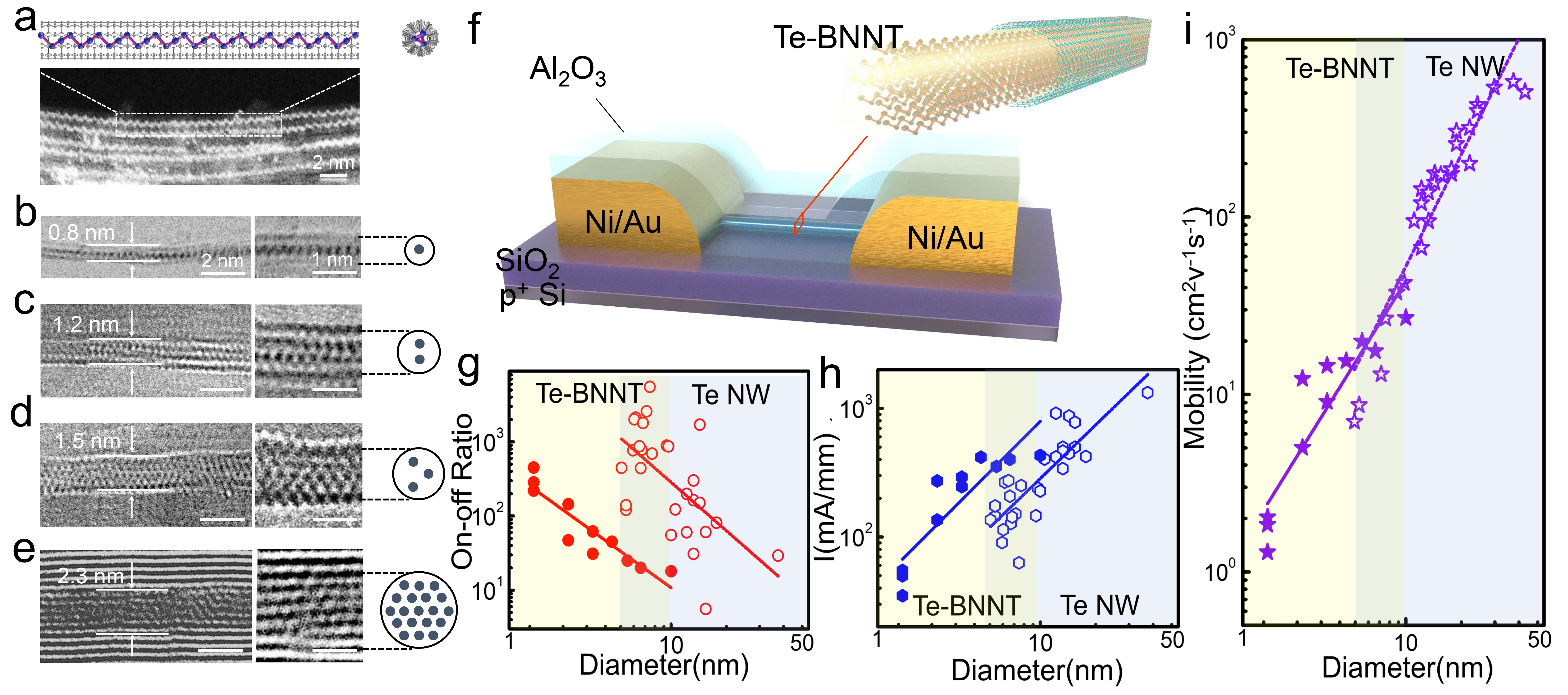
Fig. 1 | Characterization and transport properties of Te NW isolated down to few-chain limit. a, HAADF-STEM image of single Te chain in 0.8 nm SWCNT, where clear 3-fold-symmetry helical coils are distinguished. Inset image shows the corresponding schematic illustration. b-e, HRTEM images of the single, double, triple and 19 chains of Te shielded by CNT. f, Schematic of an individual Te-BNNT FET. Diameter-dependent g, on-off ratio h, current density at Vds=1 V and i, carrier mobility of Te-BNNTs and Te NWs short-channel FETs. Solid signs represent Te-BNNT NW devices and empty signs represent bare Te NW devices.
Our work demonstrated an important step for achieving high-performance FETs with atomic size and ultra-short channel beyond Moore’s law. We believe by further improving the preparation process and the quality of semi-metal contact, this technique can be well extended to other semiconductors with quasi-1D crystal structure. Besides, this prototype device based on Te-BNNT core-shell nanowire heterostructure also provides an alternative option to construct gate-all-around (GAA) FETs in the post-silicon era.
For more information, please refer to our recent publication in Nature Electronics, “Raman Response and Transport Properties of Tellurium Atomic Chains Encapsulated in Nanotubes” (https://doi.org/10.1038/s41928-020-0365-4).
Dr. Qin is currently a postdoctoral fellow in Department of Applied Physics, The Hong Kong Polytechnic University. Before that, he worked at Purdue University under a joint project from 2016 to 2018. He is a researcher in the field of nano electronics, and his studies mainly focus on low-dimensional nanomaterials and their applications for electronics, optoelectronics and neuromorphic devices.
Follow the Topic
-
Nature Electronics
This journal publishes both fundamental and applied research across all areas of electronics, from the study of novel phenomena and devices, to the design, construction and wider application of electronic circuits.


Please sign in or register for FREE
If you are a registered user on Research Communities by Springer Nature, please sign in