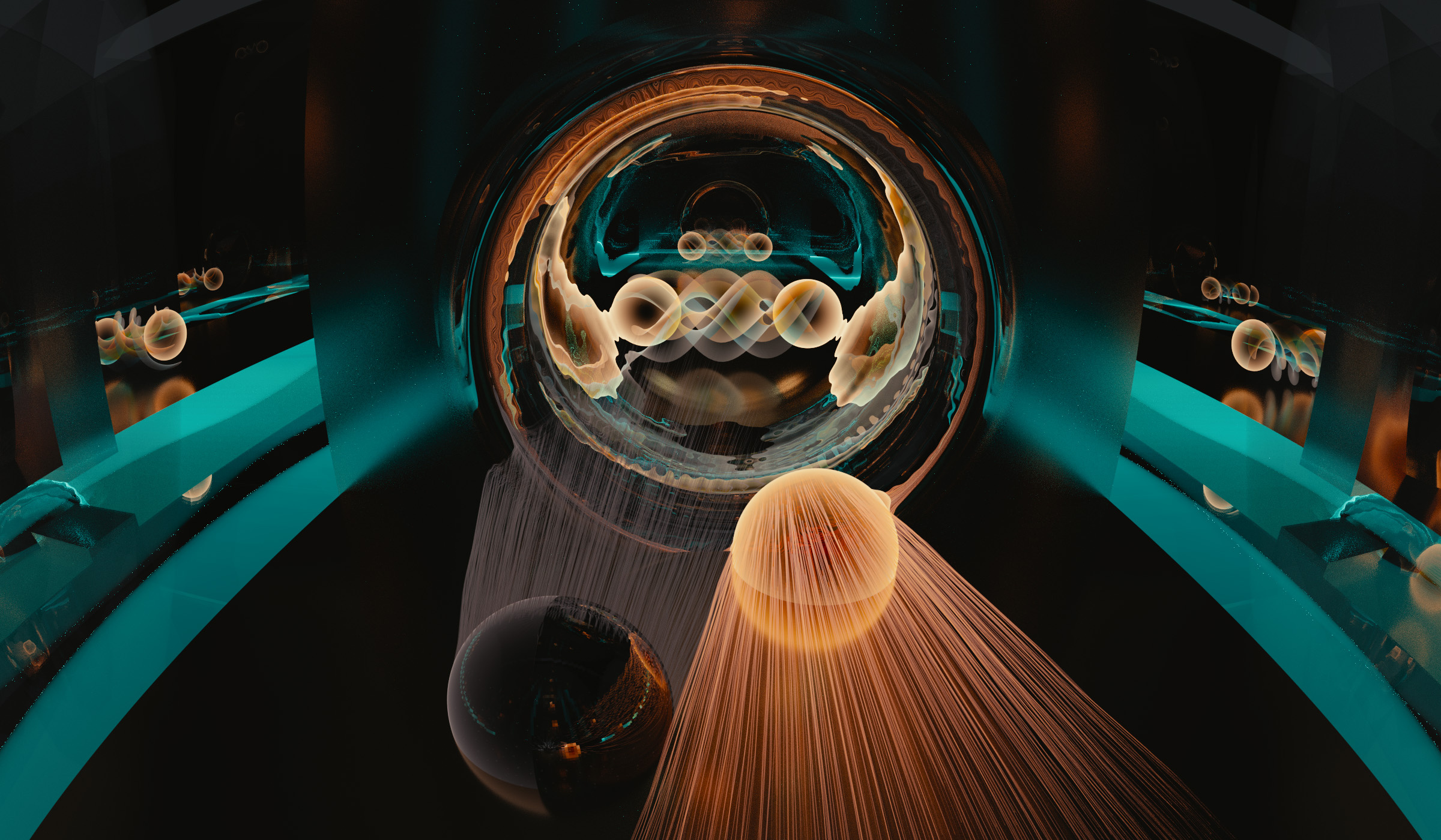
Perfect Andreev reflection due to the Klein paradox in a topological superconducting state
Published in Electrical & Electronic Engineering

When I first saw the result – perfect Andreev reflection on a topological superconducting surface state, I thought it was very strange. In fact, I didn’t believe it. After all, I have been doing point contact experiments on a variety of superconductors for over thirty years, and I have never ever seen it. So I asked Seunghun Lee and Xiaohang Zhang to repeat the experiment, and they kept coming back with the same result: the normalized differential conductance inside the superconducting gap is exactly 2 in the point contact spectroscopy on a SmB6 thin film layer proximity-coupled to a superconducting YB6 film underneath. The doubling of the conductance at a superconductor/normal metal interface, as predicted by Alexander F. Andreev originally back in 1964, is very rarely observed. In theory, one can have an ideal interface, which can result in the exact doubling, but in experiment, it is extremely difficult to achieve the “perfect” interface due to myriad reasons, e.g. natural formation of barriers and defects, materials properties mismatch, etc. Just to be sure, we have surveyed hundreds of published results on point contact Andreev reflection experiments over decades, and found only one other example of exact doubling (the origin of which is different from our current observation). Fig. 3 of our paper captures this.

It was Victor Galitski who realized that we may be observing the Klein paradox, a relativistic tunneling phenomenon theoretically discovered by Oskar Klein. Klein had solved the usual potential step problem in quantum mechanics using the Dirac equation in 1929 and found that for relativistic particles, the transmission coefficient is always unity regardless of the potential barrier height. The reason we might expect to observe such a relativistic effect in a solid material is the presence of special states at the surface of a topological insulator: the electrons in these states behave at low energies as relativistic Dirac particles. As applied to our superconducting/normal interface, this translates to perfect Andreev reflection, i.e. exact doubling of the conductance inside the superconducting gap. Valentin Stanev and Victor then soon worked out the relativistic (Dirac) version of the famous BTK (Blonder, Tinkham, Klapwijk) theory, which describes transport across superconductor/normal metal interfaces, and we quickly saw that the new Dirac-BTK theory can correctly account for all of our observations. Victor Yakovenko also played a key role in advancing our understanding of what was happening at our unique interface.
Klein tunneling had been observed before in graphene based devices, but this was the first time it was observed with a 3D topological insulator and with a superconductor. SmB6, our topological insulator of choice, is special in that it has a true insulating bulk at low temperatures, and it also has unusual 1D surface nanostructure features which are important for Klein tunneling. Johnpierre Paglione and Richard Greene had previously worked extensively with single crystals of SmB6 at the University of Maryland, and their expertise played a crucial role in designing our thin film experiments. The electron microscopy work by Xiaoqing Pang and his group members at UC Irvine was also indispensable in uncovering microstructural details of our thin film materials.
The notion that a natural tunnel barrier “disappears” due to the Klein paradox has far-reaching consequences. The Achilles heel of circuits based on Josephson junctions is the often uncontrollable variability in the tunnel barrier. In principle, if we make an array of Klein Josephson junctions, they should all have “identical” junction parameters. In a way, we have already observed this. Our Fig. 2e shows that a point contact to just a superconducting YB6 film clearly exhibits a normal tunneling behavior due to a natural barrier. When now we “insert” a thin SmB6 layer, the barrier disappears and gives rise to the perfect Andreev reflection (Fig. 1c,d).
The fact that we are able to observe perfect Andreev reflection with SmB6 indicates that we should also be able to achieve perfect spin filtering with magnetic layers. We therefore believe Klein tunneling with SmB6 thin films can be the basis for a new family of superconducting and spintronic devices whose interface transport phenomena are completely governed by their topological surface states. SmB6 thin films can be fabricated by relatively-simple RF sputtering, and therefore devices and circuits based on them can be scaled up in a straightforward manner.
For more details on our work, please see S. Lee et al. Nature 570, 344-348 (2019) (https://www.nature.com/articles/s41586-019-1305-1)
Follow the Topic
-
Nature
A weekly international journal publishing the finest peer-reviewed research in all fields of science and technology on the basis of its originality, importance, interdisciplinary interest, timeliness, accessibility, elegance and surprising conclusions.
Related Collections
With Collections, you can get published faster and increase your visibility.
Carbon Dioxide Removal
Publishing Model: Hybrid
Deadline: Jan 16, 2027


Please sign in or register for FREE
If you are a registered user on Research Communities by Springer Nature, please sign in