Potential of grayscale nanolithography for 2D nanoelectronics
Published in Materials
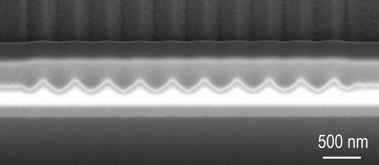
The field of nanolithography has been steadily evolving over the years, with the primary focus on downscaling the minimum feature size driven by Moore's law, enabling the fabrication of increasingly compact and powerful processors. Grayscale nanolithography extends this concept by introducing multiple depth levels within a single pattern, unlike conventional lithography that is limited to two depth levels. This ability to create 2.5D topographies with deterministic geometries has opened up new possibilities, particularly in the fields of optics, fluidics, and now in electronics, introducing new functionality in devices or improving performance.
Deterministic grayscale nanopatterning
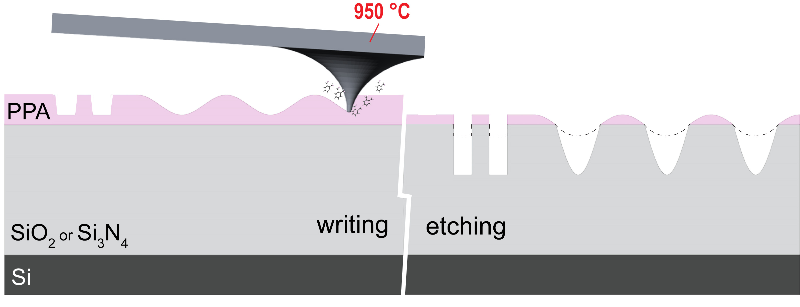
For non-binary grayscale nanopatterning, various techniques such as electron beam lithography, interference lithography, and scanning probe lithography have been explored, each with its own strengths and limitations. Among them, thermal scanning probe lithography (t-SPL), free of electron scattering and diffraction limits, stands out for its ability to achieve sub-nanometer vertical resolution and single-digit nanometer lateral resolution1. Grayscale t-SPL, creating complex surface geometries with nanometer precision using heated ultra-sharp nanotips, faces its own challenges. Two of them are limited pattern depth and low throughput. The limited pattern depth restricts the efficiency of the functional device, while the low throughput limits its scalability for mass production.
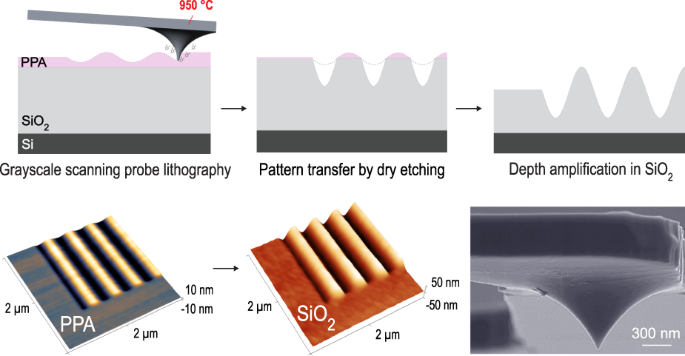
To address these limitations, we demonstrated a new generic nanoengineering process that combines single-digit nanometer precise nanopatterning in x, y, and z using t-SPL, plasma etch recipe with a He-based substrate cooling cycle for optimized etch selectivity between thermal resist and SiO2 or Si3N4, allowing for pattern depth amplification up to 10-fold and a smooth surface. This technique effectively amplifies polymer nanopatterns in thin-film dielectrics, achieving a significant increase in depth without introducing additional surface roughness. Moreover, to enhance throughput, we replicated grayscale dielectric nanostructures on larger surfaces through nanoimprint lithography, enabling the rapid production of high-quality nanostructures. Nanoimprint lithography showing equivalent surface quality control to validate the potential for upscaled manufacturing of grayscale patterns2.
Promises for the next generation of electronics: 2D materials
The emergence of grayscale nanolithography coincides with the rise of 2D materials, a new class of ultrathin materials with remarkable electric and optic properties. These materials, particularly 2D semiconductors, are extensively investigated for the next generation of nanoelectronics, as they hold the potential to replace silicon in transistors with sub-10 nm channel lengths and can revolutionize the processor industry with nanosheet stacked transistors3.
However, their full potential is hindered by inherent limitations and further fundamental studies are needed to better understand the physical and electronic properties of 2D semiconductors and their integration into current state-of-the-art processors. One of the emerging aspects being considered is strain engineering of 2D materials similar to the approach used in silicon-based transistors to improve carrier mobility. In our work, we demonstrated the effective modulation of the strain distribution by conformally adhering the 2D materials to a dielectric layer previously nanoengineered with a gray-tone topography, leading to significant improvements in carrier mobility and device performance. As an example, we showed stain modulation in monolayer MoS2, but straining of atomically thin materials on pre-structured surfaces is generic and applicable to various 2D materials, regardless of p- or n-type.
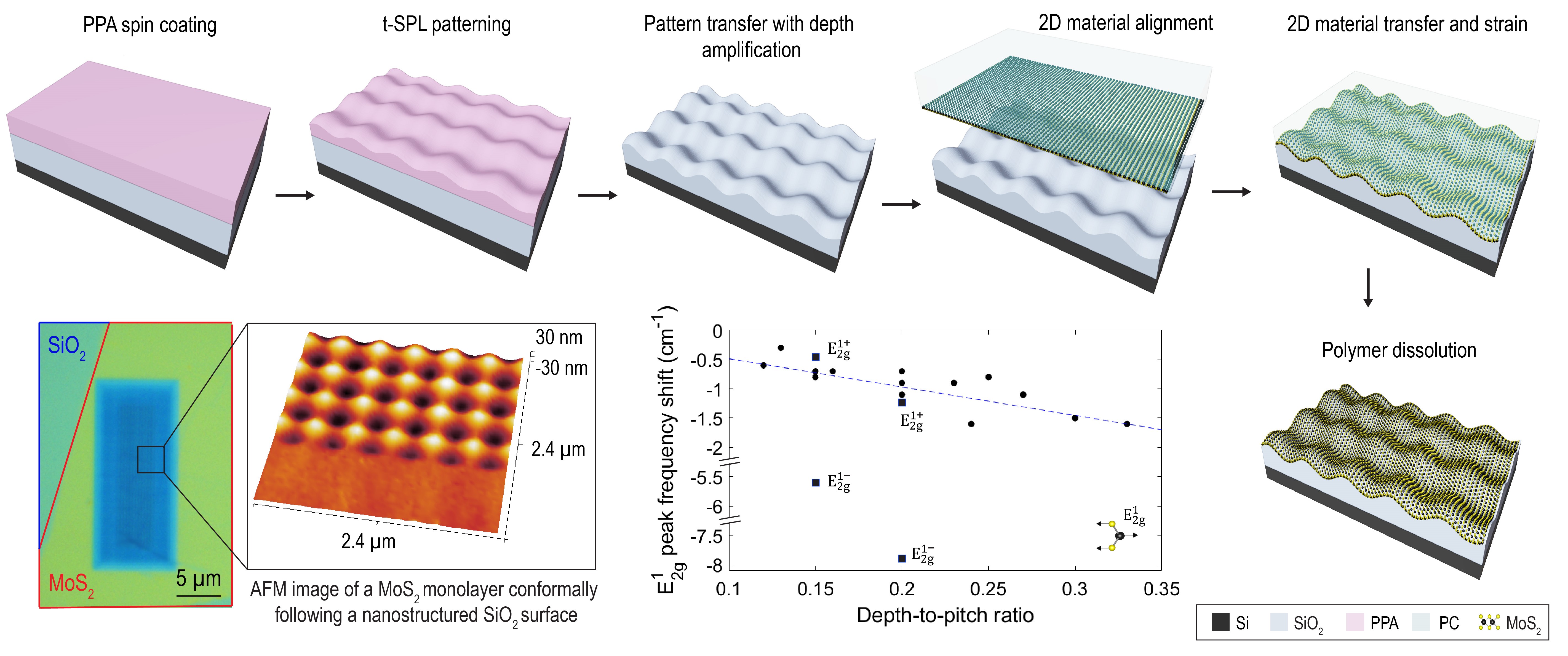
Deterministic, local, and bi-axial strain engineering in atomically thin MoS2 through 3D topographic nanopatterning
Nanolithography and strain engineering for 2D materials
The potential to customize the electronic characteristics of 2D materials using grayscale nanolithography presents significant promise for advancing the field of next-generation nanoelectronics. Grayscale nanolithography's ability to create intricate 2.5D structures and introduce precise strain adjustments may lead to a rethink of the design and manufacturing processes of electronic devices. By engineering the electronic properties of 2D materials, researchers can optimize device performance, enhance energy efficiency, and reduce device size, paving the way for a new era of miniaturized, high-performance electronics.
References:
- Howell, S. T., Grushina, A., Holzner, F. & Brugger, J. Thermal scanning probe lithography—a review. Microsystems Nanoeng. 2020 61 6, 1–24 (2020).
- Erbas, B. et al. Combining thermal scanning probe lithography and dry etching for grayscale nanopattern amplification. Microsystems Nanoeng. 2024 101 10, 1–10 (2024).
- O’Brien, K. P. et al. Process integration and future outlook of 2D transistors. Nat. Commun. 2023 141 14, 1–5 (2023).
Follow the Topic
-
Microsystems & Nanoengineering
This journal, with a target for a high-end journal for years to come, seeks to promote research on all aspects of microsystems and nanoengineering from fundamental to applied research.




Please sign in or register for FREE
If you are a registered user on Research Communities by Springer Nature, please sign in