Recent Advancements and Perspectives of Low-Dimensional Halide Perovskites for Visual Perception and Optoelectronic Applications
Published in Electrical & Electronic Engineering, Materials, and Physics

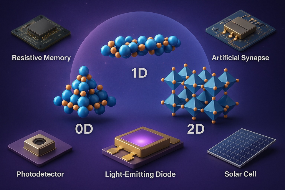
A research team led by Professors Hugo Águas and Santanu Jana has published a comprehensive review in Nano-Micro Letters which systematically summarizes the structural design, synthesis strategies, and emerging device applications of zero-, one-, and two-dimensional (LD) halide perovskites, offering a timely perspective on how dimensional engineering enables advanced optoelectronic functionalities beyond traditional semiconductors.
Dimensionality and Structure–Property Correlation
Low-dimensional halide perovskites—comprising 0D quantum dots, 1D nanowires, and 2D layered crystals—exhibit unique light–matter interactions owing to quantum confinement and anisotropic charge transport. The review highlights how compositional and structural tuning in these systems allows precise modulation of bandgap, exciton binding energy, and photoluminescence, establishing direct correlations between dimensional motifs and functional performance in light-emitting diodes (LEDs), photodetectors, and solar cells.
Synthesis and Fabrication Strategies
- Solution-phase and vapor-phase growth: Techniques such as hot injection, chemical vapor deposition (CVD), and templated synthesis have enabled scalable fabrication of LD perovskite nanostructures with controlled thickness and morphology.
- Single-crystal growth: Recent advances in interfacial nucleation and vapor diffusion methods have yielded large, high-quality 2D single crystals, crucial for defect-free charge transport and device stability.
- AI-assisted design: Machine learning and first-principles simulations are accelerating the prediction of structural dimensionality and optoelectronic properties, providing a roadmap for the rational design of next-generation perovskites.
Optoelectronic Applications
LD halide perovskites combine strong excitonic effects, high absorption coefficients, and tunable bandgaps, enabling outstanding performance in various devices:
- Light emitters and displays benefit from narrow emission spectra and near-unity photoluminescence quantum yields.
- Photodetectors and synaptic devices exploit fast carrier dynamics and high responsivity for artificial visual perception systems.
- Photovoltaics achieve enhanced efficiency and stability through Ruddlesden–Popper and Dion–Jacobson architectures with reduced ion migration and improved environmental tolerance.
Challenges and Outlook
Despite their promise, LD perovskites face limitations in environmental stability, large-area uniformity, and interfacial engineering. The review emphasizes emerging solutions such as compositional optimization, encapsulation, and green, low-temperature processing. Looking ahead, the integration of multifunctional LD perovskites into flexible, neuromorphic, and intelligent optoelectronic platforms is expected to redefine the boundaries of visual sensing and photonic computation.
By bridging structural chemistry with functional device design, this review provides a forward-looking framework for translating laboratory-scale low-dimensional perovskite innovations into scalable, sustainable optoelectronic technologies.
Editor of Nano-Micro Letters, which is an Open-Access, peer-reviewed journal reported papers that have at least one dimension ranging from a few sub-nanometers to a few hundreds of micrometers. The journal is published by Springer Nature and indexed by SCI, EI, SCOPUS, Pubmed, etc. The 2025 JCR Impact Factor is 38.5. The 2025 CiteScore is 58.9.
Follow the Topic
-
Nano-Micro Letters
Nano-Micro Letters is a peer-reviewed, international, interdisciplinary and open-access journal that focus on science, experiments, engineering, technologies and applications of nano- or microscale structure and system in physics, chemistry, biology, material science, and pharmacy.


Please sign in or register for FREE
If you are a registered user on Research Communities by Springer Nature, please sign in