Semiconducting nanotube shows photovoltaic effect without p-n junction
Published in Electrical & Electronic Engineering
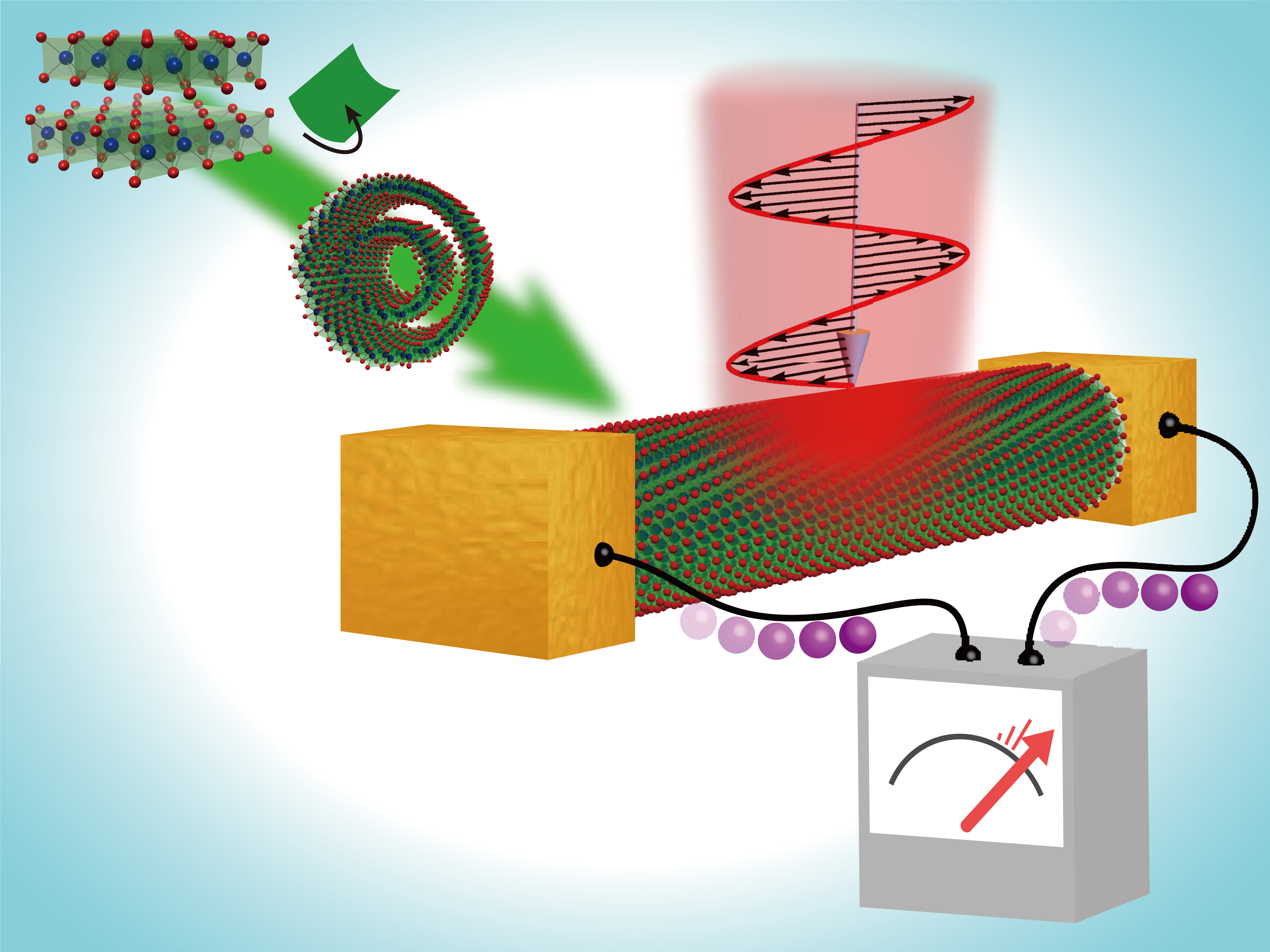
The discovery of this phenomenon was really unexpected. While my main task was to build an opto-electrical measurement facility in Max Planck Institute for Solid State Research, in the meantime I was organizing old data. I found a strange signal in one of the old back-up file of gate-depended photoluminescence (PL) measurement on tungsten disulphide (WS2) nanotubes. A tiny external bias voltage was applied to the nanotube and the current was monitored during PL measurements to track the gating effect and to ensure that the nanotube was not damaged by laser irradiation. The electrical current showed a sudden change when the laser was switched on, which seemed reasonable at first glance. Photo-excited carrier will increase the conductivity, so-called photoconductivity. Therefore, current should increase when light is switched on. However, some nanotube device showed “a sign change” upon laser irradiation; a positive current at dark while a negative current under illumination. This means that there exists another driving force to move carriers against the external bias voltage when the nanotube is illuminated.
I consulted about this phenomenon with Ryuji Suzuki, who was investigating photovoltaic effect in one kind of bulk material as his PhD project. We two together confirmed that the negative current is due to BPVE, and got very excited because this would be the first observation of BPVE in “nano”material. I knew intuitively that this phenomenon needs a timely and intensive investigation, but the construction of measurement facility in Max Planck Institute was delayed. Fortunately, Professor Yoshihiro Iwasa offered a long-term measurement slot in his group. Hence, I visited University of Tokyo and accumulated the first set of experimental data, which covers most of the figures shown in the main text.
The efficiency of BPVE in WS2 nanotube is much larger than that in other crystalline bulk materials. Although it is not yet competitive to commercial solar cells, BPVE has a “potential” to overcome it. We hope our study can inspire many scientists from various disciplines to the research field of BPVE in nanomaterials. Physicists may find this phenomenon interesting. Materials scientists may investigate other nanomaterials exhibiting BPVE. Chemists may improve synthesis procedure. Device engineers may integrate a number of nano devices into a “panel”. With all these efforts together, we hope as a long-term perspective to see a next-generation solar panels based on BPVE in the commercial market.
Follow the Topic
-
Nature
A weekly international journal publishing the finest peer-reviewed research in all fields of science and technology on the basis of its originality, importance, interdisciplinary interest, timeliness, accessibility, elegance and surprising conclusions.

Related Collections
With Collections, you can get published faster and increase your visibility.
Carbon Dioxide Removal
Publishing Model: Hybrid
Deadline: Jan 16, 2027


Please sign in or register for FREE
If you are a registered user on Research Communities by Springer Nature, please sign in