Sub‑100 Femtosecond All‑Optical Modulation Beyond Electron–Phonon Limits

Introduction: The Race for Ultrafast Photonic Computing
As global data traffic explodes, the demand for high-speed optical computing and all-optical signal processing has reached an unprecedented level. To enhance data throughput and energy efficiency in next-generation photonic circuits, researchers have long looked to plasmonic all-optical modulators. These devices can manipulate light at deep-subwavelength scales with potentially ultrafast response times.
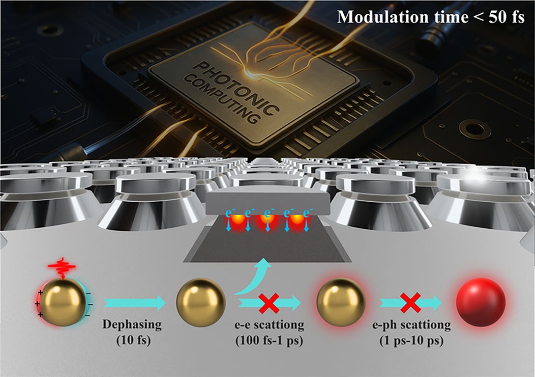
However, a fundamental speed limit exists: the "electron-phonon relaxation bottleneck". In conventional plasmonic materials, the time it takes for excited electrons to transfer energy to the material's lattice typically constrains modulation speeds to the picosecond (trillionth of a second) regime. A breakthrough study published in Nano-Micro Letters by a collaborative team from Xiamen University and Hangzhou Dianzi University provides a physical foundation for breaking this barrier, achieving modulation in the tens-of-femtoseconds range.
The Current Benchmark: Overcoming the Picosecond Tail
The primary challenge in ultrafast optics is that even when a device shows a fast initial response, it is often followed by a persistent "relaxation tail" governed by lattice heating. This tail limits both the switching contrast and the ultimate recovery speed of the modulator.
To address this, the researchers developed a silver-single-crystal silicon nanodisk antenna (SSDMA). By precisely engineering the nanostructure, they created a system where energy is not just absorbed, but is immediately "extracted" before it can heat the material's lattice.
The Synergetic Approach: Interface-Governed Carrier Dynamics
The researchers moved beyond traditional designs by integrating two key innovations:
- Interfacial Plasmonic Confinement: The nanodisk architecture spatially co-localizes plasmonic energy deposition exactly at the metal-semiconductor boundary. This markedly shortens the transport pathway for hot carriers, allowing them to reach the interface in record time.
- Nonthermal Extraction Pathway: By activating an interface-dominated electronic pathway that precedes electron-phonon thermalization, the device enables a "lossless" relaxation. This allows the transient optical response to be governed by electronic limits rather than slower thermal effects.
Roadmap to Sub-100 fs Efficiency: Results and Validation
Using sophisticated femtosecond pump-probe spectroscopy, the team demonstrated a stepwise verification of their technology:
- Step 1: Direct Observation of Femtosecond Dynamics: The team experimentally resolved modulation time constants as fast as 37 ± 9 fs. This is substantially faster than conventional lattice-mediated relaxation.
- Step 2: Electron-Blocking Proof: To prove the mechanism, researchers inserted a 30 nm aluminum oxide insulating layer to block the electron flow. Without the interface transfer, the device reverted to slow picosecond-scale dynamics, confirming that the interface is indeed the key to speed.
- Step 3: High Switching Contrast: The device achieved an on-off ratio exceeding 100, which is among the highest reported for plasmonic ultrafast systems.
Real-World Impact: Next-Gen Signal Processing
The significance of this work extends beyond basic physics. By enabling modulation on timescales comparable to intrinsic electronic limits, the SSDMA architecture paves the way for:
- Femtosecond Photonic Computing: High-speed logic gates for light-based computers.
- Temporal Optical Gating: Precise "shutters" for capturing ultrafast physical phenomena.
- Multi-Frequency Systems: The ability to achieve sub-100 fs modulation across multiple discrete wavelengths.
Conclusion and Future Outlook
The integration of engineered interfacial plasmonics with sophisticated electromagnetic-thermal modelling marks a significant advance in the field of nanophotonics. By identifying a way to bypass the electron-phonon bottleneck, the researchers have provided a manual for building the next generation of ultrafast photonic components.
As these metastructures are integrated into larger systems, the move toward sub-100 fs photonic processing is no longer a theoretical goal but a practical reality, offering a future of nearly instantaneous data processing and signal control.
Editor of Nano-Micro Letters, which is an Open-Access, peer-reviewed journal reported papers that have at least one dimension ranging from a few sub-nanometers to a few hundreds of micrometers. The journal is published by Springer Nature and indexed by SCI, EI, SCOPUS, Pubmed, etc. The 2025 JCR Impact Factor is 38.5. The 2025 CiteScore is 58.9.
Follow the Topic
-
Nano-Micro Letters
Nano-Micro Letters is a peer-reviewed, international, interdisciplinary and open-access journal that focus on science, experiments, engineering, technologies and applications of nano- or microscale structure and system in physics, chemistry, biology, material science, and pharmacy.


Please sign in or register for FREE
If you are a registered user on Research Communities by Springer Nature, please sign in