100 GHz zinc oxide Schottky diodes processed from solution on a wafer scale
Published in Electrical & Electronic Engineering

The Internet of Things (IoT) can be envisaged as billions of sensors comprising massive sensor networks, which enable a fully connected and immersive world. 5G and 6G networks will provide unprecedented speeds, bandwidth and network performance to satisfy the IoT’s increasing demands. 5G mainly covers mmWave frequencies with wider bandwidths and higher data rates than currently incumbent 4G technologies. It enables a plethora of new applications, including self-driving vehicles, virtual reality, remote surgery and industrial automation (Industrial IoT), while the upcoming -anticipated within the next decade- 6G is expected to further increase the transmission bandwidths.
In general, the sensor nodes need to be: a) battery-less and self-powered, b) able to exchange information wirelessly over longer or shorter distances, and c) fabricated at ultra-low cost, as a large number of them has to be placed on every object to realise full connectivity. These requirements can be satisfied by harnessing omnipresent radio waves that can be harvested and converted to useful electrical energy, which can then be used to power the respective sensing and processing units. Tuning the frequency of operation of these radiofrequency (RF) rectifiers allows short or long-haul communication. Fabrication cost can be lowered by using simple and inexpensive techniques with low thermal budget, while the possibility of using ultra-thin flexible substrates adds an extra merit, as they can be applied in curved conformable surfaces, for instance on skin or even hair.
Mapping the research landscape
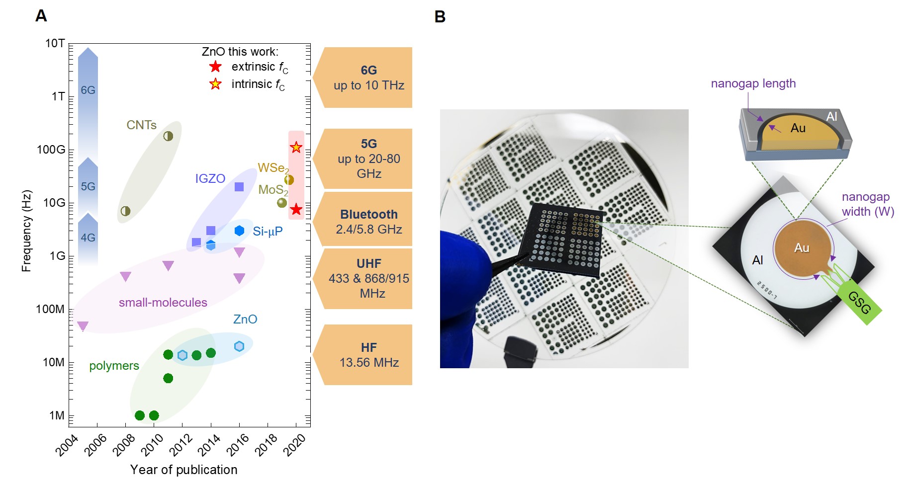
In a recent literature review article that we published (10.1088/1361-6641/aa89ce), we summarised the latest progress and current status of flexible RF diodes and rectifiers. We identified the trade-off between high performance, in terms of the devices’ highest operating (cutoff) frequency, and their potential for high throughput fabrication with large area flexible substrates. As shown in Fig. 1a, when low temperature (<200° C), soluble semiconductors are employed in conventional metal/semiconductor/metal type diodes, the operating frequency can barely exceed 1 GHz. To reach the higher frequency domains necessitated by the 5G and 6G networks, devices with extreme dimensionality, one-dimensional (1D) carbon nanotubes (CNTs) and two-dimensional (2D) monolayers of MoS2 and WSe2 are required, which are, however, still far from commercialisation due to their complex manufacturing.

The article’s breakthrough
In our Nature Electronics article we highlight the importance of combining innovative device architecture and diligent material research effort with an alternative nanopatterning technique to bridge the performance-cost gap.
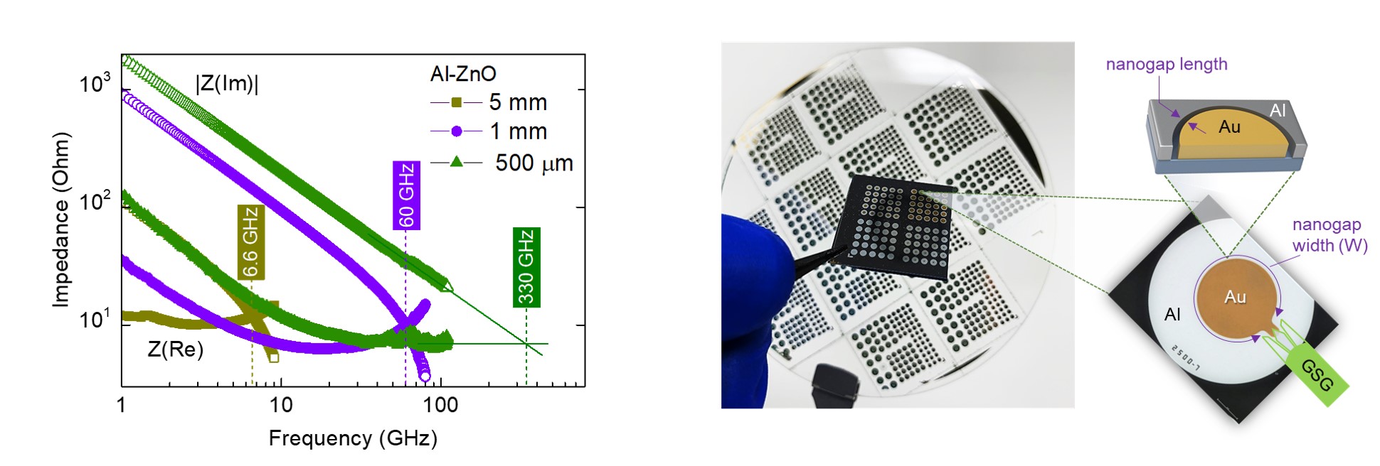
A key challenge in developing ultra-high frequency Schottky diodes is the ability to simultaneously reduce the junction resistance and capacitance, while retaining the substrate temperature during processing at low levels (<200° C). We used coplanar nanogap (≈15 nm) electrodes — a geometry that allows for significant capacitance reduction by shrinking the active layer thickness to the nanogap channel length, while maintaining the device width on the macroscale. This way we push the cutoff frequencies above 100 GHz and form diodes that can serve the 5G and potentially 6G frequency requirements.
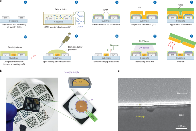
We fabricated our devices using a novel nanopatterning technique, called adhesion lithography (see also our article published in npj Flexible Electronics), that allows for high-throughput manufacturing of variable aspect ratio nanogap-separated electrodes on wafer-scale substrates (Fig. 1b). Furthermore, by meticulously doping the abundant low-cost semiconductor zinc oxide (ZnO) with Aluminium, we tune the thin film electron transport properties and demonstrate rectifier circuits that are able to operate at extremely high frequencies of tens of GHz.
Behind the scenes
Research may be a bumpy journey and for this reason it is better enjoyed when in the right company. Interdisciplinarity was key in this instance; this work was the result of a synergistic effort among three research labs (Imperial College London, KAUST and VTT), one industrial partner (PragmatIC/Centre for Process Innovation), and researchers spanning across two continents and four countries (UK, Finland, Saudi Arabia, India). A holistic approach was indispensable to first comprehend the device operation, then optimise the functional material, develop a high-frequency measurement setup that minimised noise, accurately analyse the results and finally draw key conclusions therefrom.
Our greatest technical challenge was in defining the cutoff frequency of our smallest size diodes (<500 μm width). We visited different radiofrequency electronics labs in the UK in order to ascertain what the highest performance we can obtain from our nanogap ZnO Schottky diodes is. To our surprise, even though we kept increasing the measuring range of the respective signal generator from 1 to 20 and even 50 GHz, we still could not define the cutoff frequency of the smallest size diodes. They were actually showing no losses as the frequency increased! This means their cutoff frequency was beyond our measurement range. We ultimately reached out to our colleagues in VTT, Finland, to take advantage of their ultrahigh frequency measuring capabilities (up to 110 GHz) and their technical expertise, as the noise implications and artefacts become critical when we move from MHz to GHz domain and above, owing to reflections of microwave (>1 GHz) and, more importantly, millimetre waves (>30 GHz).
After getting reliable and repeatable results in small-scale devices, we focused on proving the scalability of our technology. We collaborated with a leading UK flexible electronics company, PragmatIC, and used their facilities in the Centre for Process Innovation to demonstrate that hundreds of functional ZnO-based diodes could be fabricated with high yield (>97%) on 4- and 6-inch glass and plastic (flexible) substrates. These results testify to the enormous potential of adhesion lithography for immediate uptake by the electronics industry and its adoption as a new circuit design paradigm for Internet of Things device ecosystems based on upcoming wireless standards (5G and 6G).
You can find more details about this work in our research article published in Nature Electronics: Georgiadou, D.G., Semple, J., Sagade, A.A. et al. 100 GHz zinc oxide Schottky diodes processed from solution on a wafer scale. Nat Electron (2020). https://doi.org/10.1038/s41928-020-00484-7
Follow the Topic
-
Nature Electronics
This journal publishes both fundamental and applied research across all areas of electronics, from the study of novel phenomena and devices, to the design, construction and wider application of electronic circuits.


Please sign in or register for FREE
If you are a registered user on Research Communities by Springer Nature, please sign in
It was really great and happy about supporting this study and I am really proud about being a part of it.