3-in-1 Signal Tuning enabled by Reconfigurable FETs on 22 nm FDSOI
Published in Electrical & Electronic Engineering

Progress in nanoelectronics in the past has been overwhelmingly dominated by Moore's Law, which is the self-fulling prediction that the number of electronic components on chip will roughly double every two years for economic reasons. This prediction, made in 1965, soon became the target for the electronics industry, leading to a shrinking of the size of the individual elements, accompanied by higher individual device performance and lower power consumption. However, in recent years physical limitations have already retarded the progress of continuous miniaturization. So, one fundamental question we came up with was:
Why not cram more functions into a single element instead of cramming more elements onto a chip?
The Reconfigurable Field Effect Transistors (RFET) is a technology that enables such a solution. These devices can dynamically change their electrical characteristics from p-type to n-type functionality on request by an external electrical signal. This function is enabled by electrostatic doping using a physical design with multiple independent gates instead of the presence of impurities inside the channel. Albeit generally larger than their CMOS counterpart, many transistors can be saved on the circuit level to yield the same overall system functionality. Over the last ten years, RFETs have been intensively studied at NaMLab built on silicon or germanium nanowires as channel material. When we aimed at taking a step forward to industrial exploitation of our technology, we asked ourselves:
How can we make our unique device design work on a CMOS platform with an acceptable number of changes concerning the baseline process?
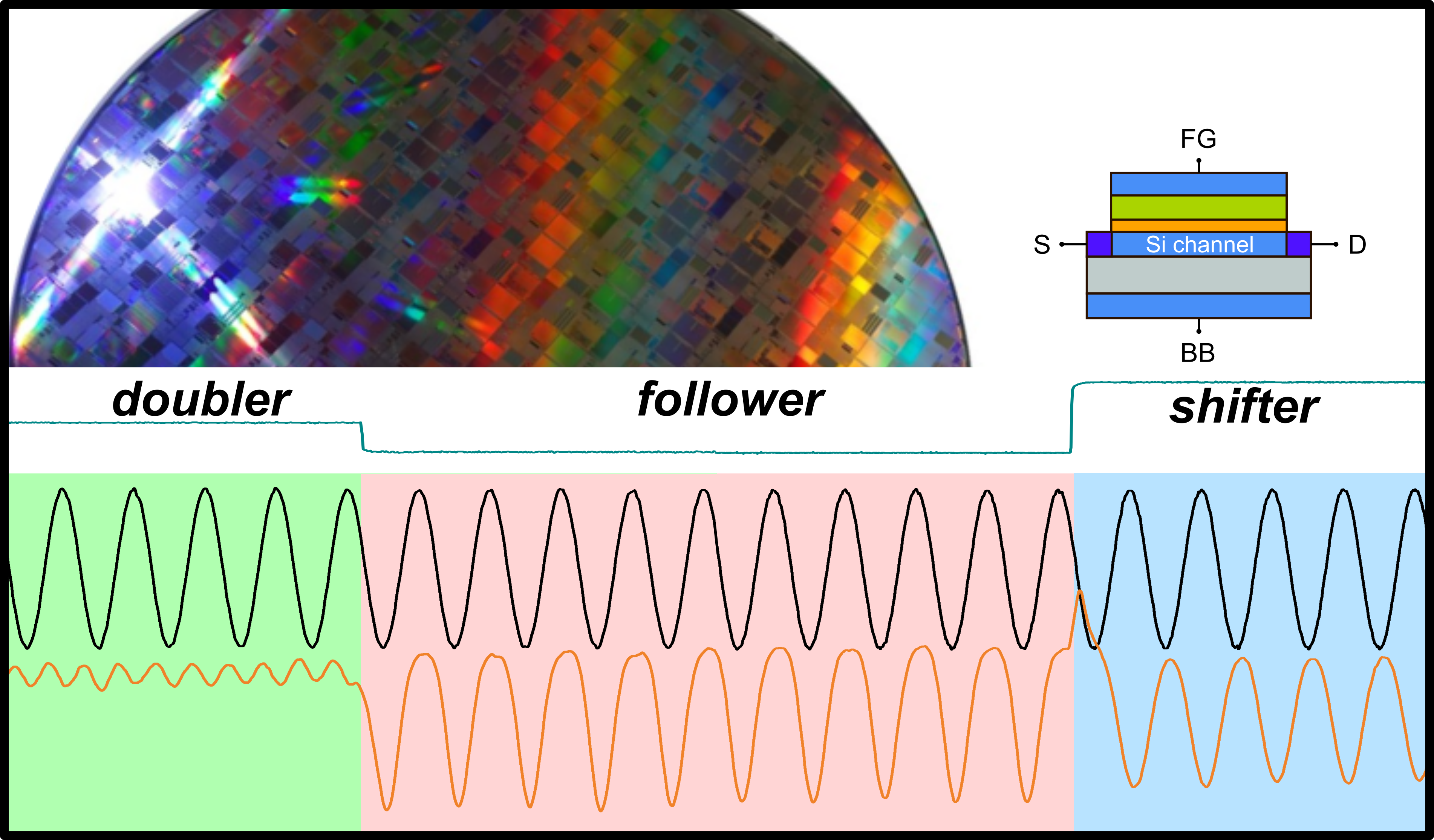
It turned out that a 22 nm FDSOI process currently run by GlobalFoundries Fab 1 in Dresden is the perfect fit for our emerging technology. The thin SOI channel already resembles the small feature sizes of a nanowire, or rather nanosheet, making sure a reasonable gate control is reached to enable barrier tunnelling. More importantly, 22 nm FDSOI provides the unique feature of body-biasing. This means the transistor can be tuned into a high-performance or low-power mode via an additional terminal at the back gate below the buried oxide. This terminal could be conveniently used as a second independent gate needed for device programming. Finally, nickel silicide, the material we needed for our barrier tunnelling, was already used to ensure contact of the source and drain towards the Back-End-Of-Line. We just needed a solution to bring the already present silicide-to-semiconductor junctions in close proximity to the doping-free channel region. This was solved by a modified source/drain contact module. All other process modules are shared with the 22 nm baseline. After integration was successfully done, the next question was:
What are the benefits of the new Back-Bias-RFET design compared to our lab designs?
Notably, the device is much smaller than its counterpart having multiple top gates. However, it only got exciting after looking into the device's electrical behaviour. Instead of having two distinct p- and n-modes, the back-bias concept can be tuned seamlessly between the two states enabling a third ambipolar mode in the middle. The nearly parabolic shape of the ambipolar transfer characteristics can be used for frequency doubling, as already shown on transistors utilizing graphene or ferroelectric hafnium oxide. The key idea now was to toggle this frequency doubling on and off by the separate back-gate signal. Three distinct modes could be selected dynamically, the frequency doubler mode, a phase follower mode, and a phase shifter mode, where the two latter keep the original frequency. The function was demonstrated with a single device element without the need for hard-to-integrate inductive elements. We believe the concept has great potential for applications in mixed-signal processing, sensing, hardware security, and maybe even data transmitters. So, there is one final question to ask:
Who will design the best circuit utilizing our 3-in-1 signal tuning enabled by Reconfigurable FETs on 22 nm FDSOI?
Read the full paper, available open access here: https://rdcu.be/cZUu1
Follow the Topic
-
Nature Communications
An open access, multidisciplinary journal dedicated to publishing high-quality research in all areas of the biological, health, physical, chemical and Earth sciences.
Related Collections
With Collections, you can get published faster and increase your visibility.
Women's Health
Publishing Model: Hybrid
Deadline: Ongoing
Biosensing
Publishing Model: Hybrid
Deadline: Jun 30, 2026


Please sign in or register for FREE
If you are a registered user on Research Communities by Springer Nature, please sign in