A Multifunctional Device Based on Graphene/Silicon Heterojunction
Published in Electrical & Electronic Engineering

In the past two decades, the variety of 2D materials with unique electrical and optical properties has been continuously enriched. Atomic-level thickness and no dangling bond on the surface make them easy to integrate heterostructures, which has made the exploration of 2D/2D and 2D/3D heterojunctions widely studied. Heterojunctions usually have inherent optoelectronic and rectifying properties, and are used to implement various functions, such as gas sensor, photodetector, solar cell, rectifier, barristor, and so on. Although the function research based on heterojunction devices is widely distributed in optoelectronics, environment, and logic electronics, not many works focus on realizing multifunctional integration in a single heterojunction device. Nowadays, the development of new technologies such as smart homes, smart cars, and smart cities put forward higher requirements for integration and multi-functionality, devices with only a single function are not competitive in modern technology. Developing a single unit that integrates multiple functions to reduce integration complexity and save costs is of great significance for the smart industry in the future. Graphene (Gr) is one of the earliest researched materials in the 2D material family. It exhibits semi-metallic properties, and its electron mobility can exceed 1.5×104 cm2·V−1·s−1, with high electrical conductivity. At the same time, the monolayer Gr has good light transmittance in a wide wavelength range due to the about 0.34 nm thickness and the 2.3% absorbance. In addition, in recent years, the fabrication of large-scale, singlecrystal domain Gr films by CVD has been intensively studied. Compared with other 2D materials, large-area growth of Gr has become possible. And in the current industry, the large-scale wafer production process of silicon (Si) based devices is highly matured. Thus, among the many heterojunction choices, Gr/Si heterojunction based device has the development foundation for large-scale fabrication in the near future. In this work, a multifunctional device based on Gr/Si heterojunction is proposed, which can achieve a low off-state current (10−8 A), high responsivity photodetection, and the response is tunable by the external electric field. At Vg pulse of 30 V and Vds of −2 V, the responsivity can be 51 A/W and 495 A/W at 266 nm and 532 nm illumination. Besides, it can also function as a tunable rectifier in logic circuits. The rectifying direction can be reversed by gate voltage, which has potential application prospects in signal processing units and tunable logic gates.

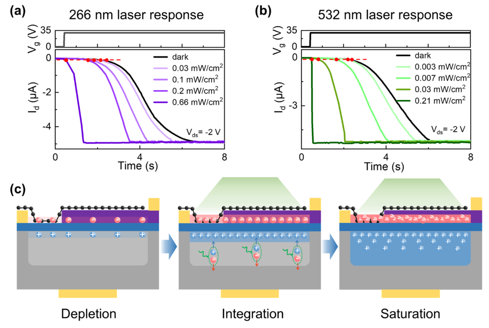
A Vg pulse with an amplitude of 30 V, period of 8 s, rise time of 15.1 ms, and duty ratio of 95% is applied at the back gate. The response of Id with time under different intensities of 266 nm and 532 nm laser illumination are shown in Fig. 3(a) and (b). During the Vg = 0 V period, the device operates in the off-state, and the off-state current is 10−8 A. At the moment of the Vg pulse amplitude from 0 V to 30 V, the device changes from off-state to on-state, and Id gradually increases with time. Since a certain number of electrons is required for the “on” of the Gr/Si heterojunction channel, a “threshold time” can be observed before Id rapidly increases, as shown by the red dots in the Fig. 3(a) and (b). As the light intensity increases, the number of electrons increases faster, and thus the “threshold time” gradually decreases. After the “threshold time”, Id enters a rapid increase phase and finally Id will reach saturation.
The stronger the light intensity, the faster the photogenerated holes fill the deep-depletion region, and the earlier Id reaches saturation. Therefore, the current in the dark and the light can be obtained by sampling at a specific time in the rapid increase phase, and the difference is the photocurrent. It is clear that the photocurrent increases as time increases because of the photocharge integration effect in the deep-depletion region. Thus, the maximum responsivity can be obtained when the sampling time is selected as the moment Id reaches saturation. According to the I-t curves in Fig. 3(a) and (b), the responsivity of the device at saturation moment can be 51 A/W and 495 A/W under 0.2 mW/cm2 266 nm laser illumination and 0.007 mW/cm2 532 nm laser illumination, respectively, indicating the photoresponse of the device can cover the ultraviolet to the visible. We compare our device’s off-state current and responsivity (UV and visible) with some reported graphene/silicon based works, as shown in Table I. The performance of our device is comparable to many reported photodetectors. Traditional graphene/silicon heterojunction devices are usually photodiode structures and lack an internal gain mechanism, causing the responsivity to be often lower than 1 A/W. But in our device, photocharge integration in the deep-depletion region helps to improve the photoresponse as integration time increase, which enables the device to have a large photoresponsivity.
Fig. 3(c) shows the operation mechanism of the device at on-state. A deep-depletion well is formed in the substrate due to the Vg pulse. In dark conditions, only thermally generated minority carrier holes are integrated under the electric field at the BOX/substrate interface. Electrons are induced in the top Gr/Si heterojunction due to field-effect, which changes the carrier concentration in Gr and top Si and affects the barrier height of heterojunction, contributing to the change in current. But when the device is illuminated, the Si substrate absorbs the photons to generate electron-hole pairs, not only thermally generated but also photo generated holes are integrated, thus increasing the speed of filling deep-depletion well. The band diagrams of the device are shown in Fig. 3(e) and (f). As the deep-depletion well is filled with holes, the induced electrons in the heterojunction no longer increase, and the current reaches saturation.
It is worth noting that the long time needed for Id to reach saturation in Fig. 3(a) and (b) is not the response time of the device but the integration time to fully fill the deep-depletion well. The response time of the device can be seen in Fig. 3(g), which shows the device follows the change of a fast switched laser illumination at a time scale < ∼20 μs. Consequently, we can infer that the response time should be much shorter than 20 μs.


Please sign in or register for FREE
If you are a registered user on Research Communities by Springer Nature, please sign in