Current Crowding in Graphene-Silicon Schottky Diodes
Published in Electrical & Electronic Engineering

In this work, we investigated the dominating and limiting factors of Gr/Si interfaces designed for high light absorption, paying particular attention to the nature of the contact failure under high electrostatic discharge (ESD) conditions. Our results indicated that current crowing (CC) is the dominant source of device failure in graphene-based devices. Current crowding caused by highly electrostatic fluctuations at the 2D/3D interfaces significantly limits the device lifetime and performance. Reducing the current crowding effects at the contact edges of graphene by engineering device structure can substantially enhance the current density (up to ~5x10³ A/cm2) and breakdown voltages (forward/reverse ~100/181V) of Gr/Si Schottky junctions. Benefitting from broadband photodetection and Gr/Si junction robustness, it may find excellent potential for applications where high current carrying capability and avalanche photodetection at significant high voltage biases are desired.
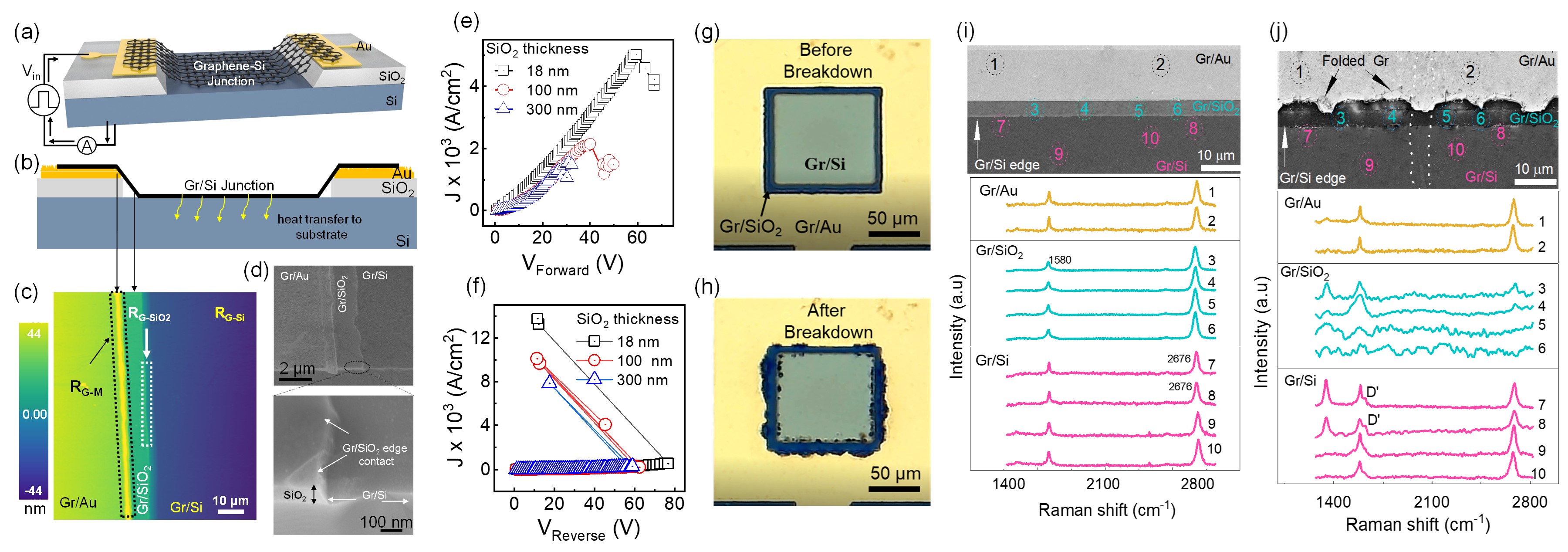
The 3D schematic of the Gr/Si Schottky junction is presented in Figure 1(a). The cross-sectional and AFM images are presented in Figures 1(b) and 1(c), respectively. The AFM image shows four regions of measurements for surface roughness evaluation, such as graphene-metal lateral and edge contact (RG-M), suspended graphene region (RG-SiO2), and Gr/Si (RG-Si) interface, showing a visible distinction in surface roughness. The roughness of the junctions is graphene-metal (RG-M) = ~4 nm (lateral), ~35 nm (edge site), RG-SiO2 = ~10 nm, and RG-Si = ~3 nm. The AFM result shows significantly large roughness at the edge contact of Gr/metal and Gr/SiO2 region. The graphene over the transition region before breakdown is displayed in SEM images shown in Figure 1(d).

Figure 1. (a) 3D schematic of Gr/Si Schottky diode. (b) The cross-sectional image indicates Gr/Si contact area as a vertical heat sink and the suspended graphene near the contact edges. (c) AFM image of contact areas of Gr/Au (lateral and edge), Gr/SiO2 (edge), and Gr/Si. (d) SEM image of the device before breakdown. Electrical characterization of Gr/Si junction under ESD conditions. Transmission line pulse (TLP) provides the required ESD conditions with (e) forward breakdown and (f) reverse breakdown characteristics for Gr/Si Schottky diode with different SiO2 layer thicknesses. A transition from soft to hard breakdown with increasing voltage is visible through optical microscopy images of Gr/Si Schottky devices regarding a sequence of device stressing under TLP pulses before breakdown (g) and after breakdown (h) electrical stress with rising times (10 ns) and pulse widths (100 ns). SEM images and Raman spectra of Gr/Au, Gr/SiO2 and Gr/Si contacts (i) before and (j) after breakdown, respectively. The D and D՛ peaks indicate disorder, which gradually increases and becomes prominent with an increase in electrical stress. Conversely, the D, G, and 2D peaks weaken, and graphene ruptures at the edge contact (points 3-6), reducing carbon atoms after an electrical breakdown.
Interfacial defects at graphene-metal contact often compromise the current carrying capability of the device and the switching speed. When the excessive heat is not dissipated properly, it accumulates in channel material leading to the device breakdown. A part of the excess energy gained by electrons from an external source (e.g., an electrical bias) is transferred to the lattice via phonon emission and subsequently increases the lattice temperature due to Joule heating. Therefore, heat mitigation is essential in graphene-based devices where the heat sink via the underlying substrate plays a crucial role. Here, we experimentally investigate the role of different contact edges that lead to the CC effect under electrostatic fluctuations for different oxide thickness.
We executed TLP testing with a sharp rise time of 10 ns and pulse width of 100 ns. The TLP test is a standard approach to ensure device reliability and stability under ESD stress. The reported devices with an oxide thickness of 300, 100, and 18 nm were tested for TLP pulses with forward-biased mode to observe current bearing capability and saturations under high electrostatic fluctuations. We observed a high current density of 5×10³ A/cm2 and improved breakdown voltage when oxide thickness beneath Gr/Au edge contact was reduced to 18 nm, as illustrated in Figure 1(e). The stress accumulation and defect generation are more severe at high ESD, which produces hotspots and localized heating at contact corners due to field crowding. Therefore, it is important to consider thinner oxide thicknesses to extend the device breakdown in large surface area Gr-Si junctions, especially for optoelectronic applications. Intrinsically, the Gr/Si Schottky junction possesses a low dark current in reverse mode and a high on/off ratio suitable for a fast Gr/Si Schottky photodiode. The reverse bias TLP testing justifies the low leakage current resulting in a large breakdown voltage, demonstrating the device ability to withstand high-amplitude ESD spikes presented in Figure 1 (f).
The excessive charge movement across the junction introduces a heating effect along the graphene channel. It is observed that the heat is appropriately mitigated where graphene is laterally contacted with metal and substrate. The graphene near the edge contacts appears to be more resistive, less efficient at managing heat, and prone to device failure. The stress accumulation and defect generation are more severe at high ESD, which produces hot spots and localized heating at contact corners due to field crowding. Furthermore, with the increase in electrical stress, the defects/cracks grow further, which melts metal electrodes and results in device breakdown (from soft to hard), as presented in Figures 1(g-h). Figure 1 (h) shows a complete breakdown with no conductive path available from graphene on Si to a gold electrode. It is clear from the optical images that the failure regions are mostly confined to Gr/Au and Gr/SiO2 edges but show a minor impact on the Gr/Si junction.
In addition, we performed the SEM and Raman microscopy of three different functional regions of the device marked as Gr/Au, Gr/SiO2, and Gr/Si to determine the exact site of graphene degradation, which subsequently led to device failure as presented in Figure 1 (i) and (j). Functional region 1: Graphene is laterally connected with Au and forms an Ohmic junction which appeared to be highly efficient in charge transfer. The non-homogenous current distribution at edge contact of Graphene/Au contributes to current crowding and hence limits the device's performance. Functional region 2 comprises edge contact and a suspended part of graphene. The high current density generates localized resistive heating at the edge contact due to current crowding and suspended regions due to the absence of heat-sinking bottom substrate, and therefore found to be less efficient in managing the heat. Functional region 3: This region is associated with the Gr/Si Schottky junction, where the generated heat is uniformly distributed owing to efficient out–of–plan charge transfers and stable junction characteristics with small Joule heating observed.
Raman spectroscopy is an appropriate characterization tool for evaluating the atomic scale disorders and defect density in a particular material. To validate the abovementioned phenomenon, we measured Raman spectra for 10 distinct regions that encompass the Gr/Au (1-2), Gr/SiO2 (3-6), and Gr/Si (7-10) to probe the material degradation under high electrical stress. In Figure 1(i) at positions 1-10, the SEM and Raman spectra show the high quality monolayer graphene with high I2D/IG > 2 and low ID/IG < 1 peak ratios. The D-band corresponds to scattering from local defects or disorders in graphene, and the G-band originates from the in-plane tangential stretching of the C−C bonds in the graphitic structures. The catastrophic effect of electrical breakdown occurs under high electrical stress as demonstrated in Figure 1 (j). Our results indicate that such failure occurs due to excessive phonon vibrations resulting in breaking the C-C bond that electrically disconnects the graphene in the device. The Raman spectra of the positions from 3-6 conclude that extensive current activity boosted the heating effects at the edge contact, resulting in material disconnection from electrodes. At positions 7-8 in the SEM image shown in Figure 1(j), the 2D peak appears at 2690 cm-1 with an emerging D′ adjacent to a high D peak at 1620 cm-1 and 1350 cm-1, respectively, owing to graphene self-rolling back (folding) after covalent bond breaking. In contrast, graphene retains its continuity and symmetry at the Gr/Si junction as represented at positions 9-10.
Finally, this work enlists the robustness and limitations of Gr/Si junction in photodiode architecture under high ESD conditions that can be used as general guidelines for 2D-3D electronic and optoelectronic devices. Benefitting from broadband photodetection and Gr/Si junction robustness, it may find excellent potential for applications where high current carrying capability and avalanche photodetection at significant high voltage biases are desired. Finally, our investigation also draw attention to the significance of improving and engineering 2D-3D interfaces to realize high-performance devices for future applications.


Please sign in or register for FREE
If you are a registered user on Research Communities by Springer Nature, please sign in