Highly Sensitive MoS2 Photodetector Based on Charge Integration and Field-Coupled Effect
Published in Electrical & Electronic Engineering

The mechanism of field-coupled effect and the photoresponse properties of the devices have been demonstrated and evaluated. Due to the strong absorption and photon-charges integration by deep-depletion region in a lightly doped silicon substrate, the strong field-coupled effect by few-layer MoS2 channel, and the effective carrier collection by monolayer graphene (Gr) electrode, the proposed MoS2-based photodetector exhibits an ultrahigh responsivity of 7.5 × 10⁴ A/W and achieves a compromise between responsivity and response speed. The deep-depletion effect triggered by pulse gate voltage enables effective manipulation and high linearity. A comparison with Gr channel shows the advantage of MoS2 photodetector in suppressing the reset current and reducing static power consumption to ∼0.1 nW. This work provides a new route for improving the performance of TMDs-based photodetectors.
Photodetectors can convert the information stored in light into electrical signals, which are crucial in our modern daily life for image sensing and optical communication. The 2-D nanomaterials have drawn increased research attention in the field of photodetection due to their unique electronic and optical properties. Among them, graphene (Gr) with a zero bandgap can be used as a transparent electrode with excellent electronic conductivity and high optical transparency. Meanwhile, molybdenum disulfide (MoS2), one of the transition metal dichalcogenides (TMDCs), has been widely studied due to its advantages, such as favorable mobility, tunable bandgaps controlled by the number of layers (1.8–1.2 eV, from monolayer to bulk), and mechanical flexibility. Intuitively, limited by the thickness, the light absorption of ultrathin MoS2 is hard to be comparable with traditional thin-film semiconductors. Nevertheless, the ultrathin thickness enables good electrical tunability by gate controlling and performance improvement by localized fields
Pristine MoS2 phototransistor relies on the photogating effect induced by trap states for modulating the channel conductance, which easily achieves high responsivity through trap-induced long carrier lifetime. However, these traps are usually difficult to precisely control and result in a nonnegligible long response time in the range of several seconds or more. Some approaches have been reported for boosting the performance of MoS2 photodetectors, such as chemical doping, surface functionalization, and hybrid heterostructures formation. However, most of the approaches still suffer from the shortcoming of compromise between response speed and responsivity. Interfacial gating effect has been reported based on the Gr-oxide–silicon (Si) structure, which can bridge the gap between ultrafast response and ultrahigh responsivity. By physically separating the photosensitive Si and Gr channel, the accumulated photocarriers at the interface gate the Gr and introduce a high gain in photoresponse as well as fast response. However, the low ON/OFF ratio and large dark current of Gr arising from the absence of an intrinsic bandgap hamper the practical circuit applications.

In this work, we report a novel MoS2-based photodetector, assisted with the electric contact of monolayer Gr and photoncharges integration in the Si substrate. A pulse gate voltage is applied on the lightly doped substrate as the drive signal in order to form a deep-depletion region, where photo-charges generate and integrate. Due to the strong field effect of MoS2 and effective carrier collection of Gr electrodes, the integrated carriers can be amplified and directly read out through the MoS2 channel by capacitive coupling. Besides, the moderate bandgap of MoS2 helps to suppress the reset current and reduce the static consumption. This charge integration and field-coupled effect enables our device to realize high responsivity, high linearity, and fast response time.
The schematic of the device structure and test circuit for the proposed photodetector is shown in Fig. 1(a), which contains the readout layer and photosensitive layer. Different from traditional 2-D field-effect transistors (FETs), we used a lightly doped Si substrate for light absorption and charge integration, which will be discussed in the following section. Fig. 1(b) shows the optical microscope image of the readout layer of a representative device based on the Gr–MoS2–Gr lateral heterojunction structure. To prove the species and structures of the materials, the Raman spectroscopy was performed for the MoS2 region and Gr electrode region, as shown in Fig. 1(c). The MoS2 film exhibits two typical signal peaks at 385 and 406 cm−1, which correspond to the in-plane E1 2g and outof-plane A1g vibrational modes, respectively. The frequency difference of ∼21 cm−1 proves the ultrathin MoS2 layer (≤3 layers). The Raman spectrum of Gr on SiO2/Si has a negligible D peak and a singlet 2-D peak, along with the intensity ratio of 2-D to G peak larger than 2, confirming the high crystal quality of the monolayer CVD Gr. The electrical transport properties of traditional MoS2 FETs are often limited by the large contact resistance at MoS2/metal interfaces. One of the methods to decrease contact resistance is using Gr as the electrodes. Fig. 1(d) shows the output characteristics of the Gr-contacted MoS2 back-gated FETs. The Vds regime from −1 to 1 V is linear without an inflection point, which suggests that Gr provides efficient contacts to the conduction band of MoS2 for electron injection.
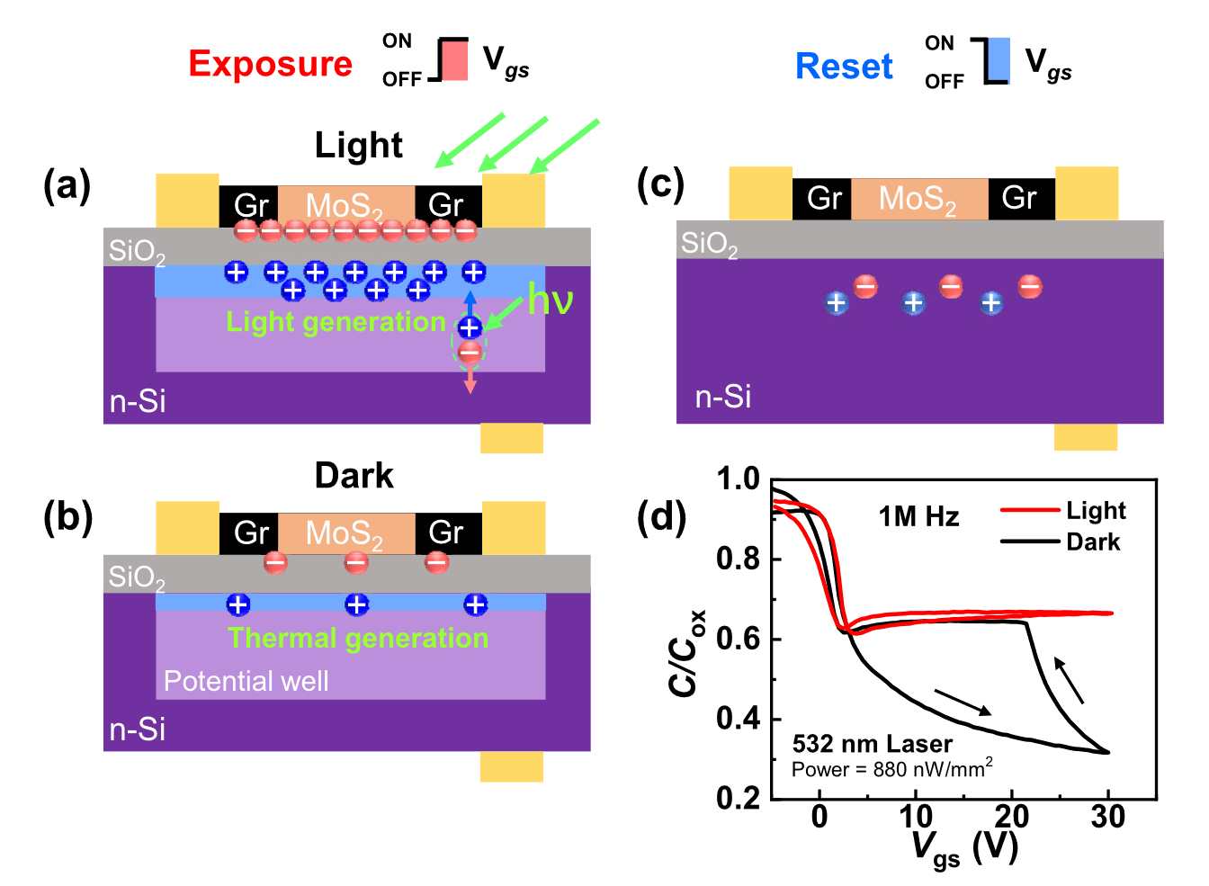
Fig. 2(a)–(c) shows the operation mechanism of fieldcoupled effect. During the exposure operation, positive pulse gate voltage (Vgs) drives the lightly doped Si into nonequilibrium deep-depletion state, a potential well is formed in the SiO2/Si interface for photon absorption and charge integration. At the same time, the corresponding electrons are coupled in the readout layer, affecting the conductivity of MoS2 channel. Under light illumination, the photo-excited electron–hole pairs will be separated by the strong electric field, resulting in positive charges accumulation in the potential well, whereas in the dark condition, there are no carriers that fill the potential well except for those from the thermal carrier generation. The slow thermal generation rate in Si keeps the state of deep depletion for a long time. In addition, the Vgs OFF signal empties the potential well and drives the Si back to the equilibrium state, switching the device to a reset state, ready for the next exposure cycle, as shown in Fig. 2(c).
The deep-depletion formation can be confirmed by highfrequency C–V measurement, as shown in Fig. 2(d).Gate voltage Vgs, defined to be positive on Si, was swept from –5 to 30 V and then swept back at a fast sweeping ramp. Under dark conditions, the continually decreasing capacitance indicates the nonequilibrium deep-depletion state. With strong light illumination, the photocarriers quickly fill the deepdepletion well, bringing the substrate back to an equilibrium state. Hence, for Vgs > ∼2.5 V, most of the electric field is applied to the oxide insulation layer, and the capacitance remains the same.


Please sign in or register for FREE
If you are a registered user on Research Communities by Springer Nature, please sign in