Active spatial control of graphene plasmons
Published in Electrical & Electronic Engineering

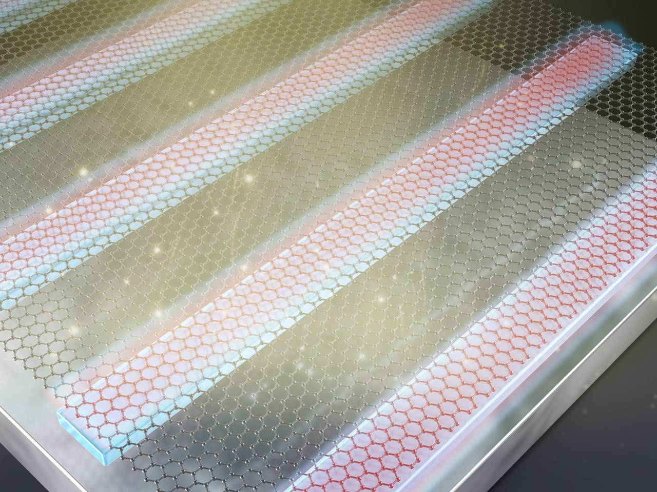
For plasmonic applications, graphene has potential advantages over noble metals owing to its relatively low loss, high confinement, and tunability by external electric field. Frequency tuning of plasmonic cavities has been demonstrated in a variety of graphene or graphene-metal hybrid structures. Beyond the frequency tuning in mechanically defined structures, it is possible to control spatial distribution or propagation direction of plasmons by tailoring spatial carrier density profile in a continuous graphene sheet. This will enable us to develop programmable plasmonic circuits. This concept is rather simple but its experimental implementation is not as straightforward as naively expected.
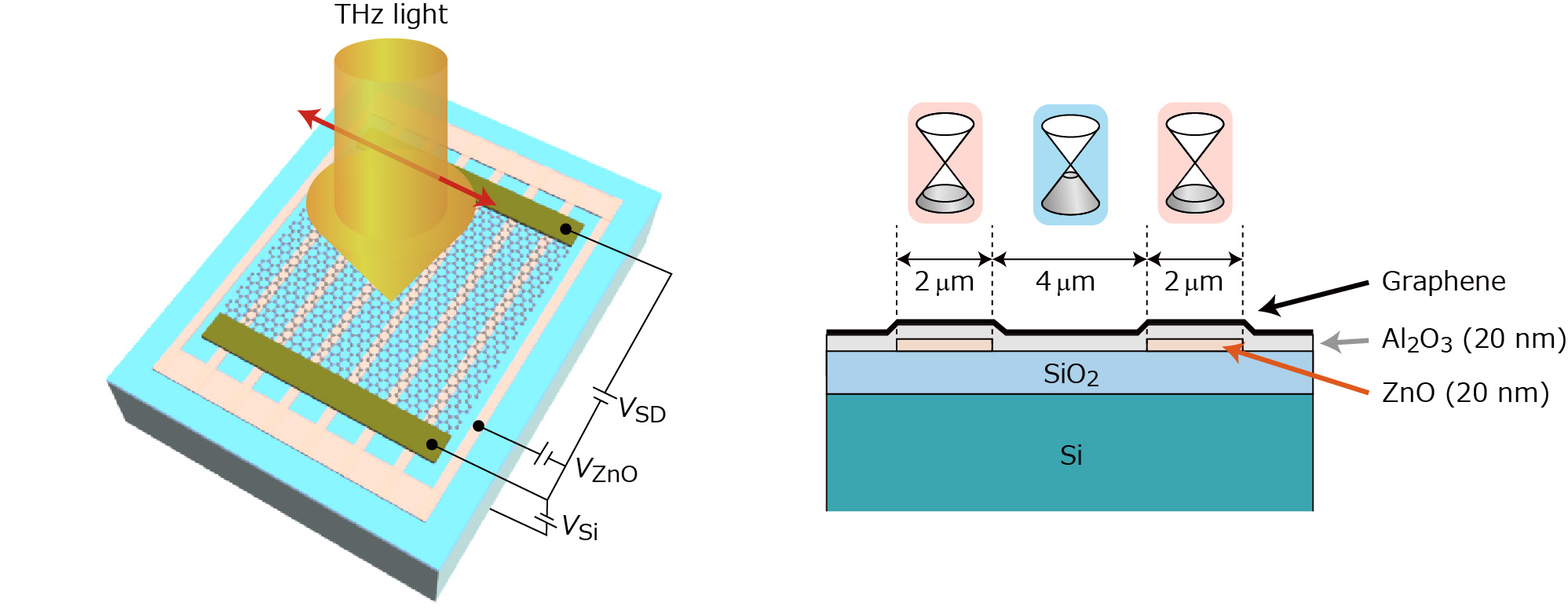
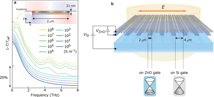
To control carrier density profile in an active manner, electrical gates are ineluctable. However, gate metals change electromagnetic environment, which induces uncontrollable plasmon reflection at gate boundaries. We tackled this issue by selecting low-conductive zinc-oxide (ZnO) thin film as a gate material. The growth temperature (180°C) of the ZnO film was carefully chosen so that the conductivity was low enough for avoiding gate screening effect in the THz range while not too low as a gate electrode. The transparency of the ZnO film is about 90% over the whole frequency range of interest between 1.3 and 10 THz. Using a dual-back-gate structure consisting of the patterned ZnO gate and a lightly-doped semi-transparent Si substrate (Fig. 1), we controlled the carrier density profile in graphene. Plasmon reflectivity at electronic boundaries between two graphene regions with different carrier density was deduced from the extinction spectra obtained by Fourier transform infrared spectroscopy (FTIR) at room temperature in the vacuum.

We demonstrated that the plasmon reflectivity at an electronic boundary can be tuned continuously from zero to a large value by adjusting the carrier density difference across the boundary. The plasmon reflectivity vs carrier density difference can be well explained by a simple model. Based on this functionality, we showed that it is possible to confine plasmons into desired regions. These results indicate that our device structure can be a platform for implementing a programmable plasmonic circuit.
For more information, please see our recent publication in Communications Materials: Active spatial control of terahertz plasmons in graphene (https://www.nature.com/articles/s43246-019-0002-9)
Follow the Topic
-
Communications Materials
A selective open access journal from Nature Portfolio publishing high-quality research, reviews and commentary in all areas of materials science.
Related Collections
With Collections, you can get published faster and increase your visibility.
Materials for quantum sensing and computing
Publishing Model: Open Access
Deadline: Jul 09, 2026
Triboelectric nanogenerators for energy harvesting
Publishing Model: Open Access
Deadline: Jun 30, 2026


Please sign in or register for FREE
If you are a registered user on Research Communities by Springer Nature, please sign in