Analogue two-dimensional semiconductor electronics
Published in Electrical & Electronic Engineering

After our demonstration of the successful two-dimensional (2D) microprocessor, we started thinking on what would be the next interesting implementation of 2D electronics and found that the area of analogue electronics with 2D semiconductors is still poorly covered. Many people have heard about digital electronics, while its counterpart, analogue electronics, stays in shadow in modern research. Despite that, it is almost as ubiquitous as digital electronics, since many electronic devices contain numerous analogue components. The basic building block of analogue electronics is the operational amplifier (opamp), a high-gain electronic component with a differential input and single-ended output that amplifies the difference in potential at the inputs with a very high gain factor. The opamp is used to build different kinds of circuits. By using a negative feedback the characteristics of the amplifier, its gain, impedance and other parameters can be tuned by external components with very little dependence on the internal parameters of the opamp itself. By using these feedback circuits, numerous functionalities can be implemented using the same opamp, ranging from simple amplifiers, to more complex systems like adders, integrators, buffers, filters and many more.
Modern analogue electronics is nearly exclusively made from silicon. However, the ever pushing demand regarding integration and diverse applications has pushed the research towards alternative materials in the same way as in the digital electronics area. Due to the improved electrostatic control, mechanical flexibility and intrinsic small thickness, semiconducting transition metal dichalcogenides (TMDs), such as molybdenum disulphide (MoS2), show great promise.

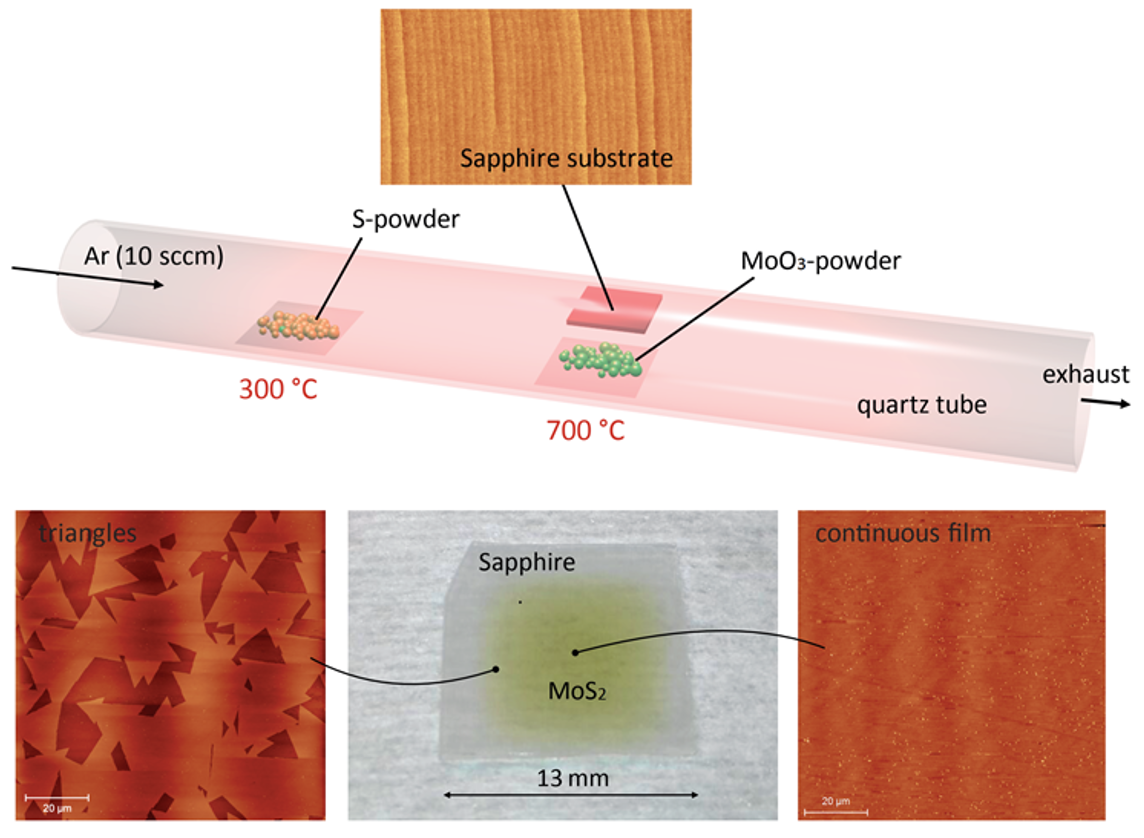
Figure 1. Schematic of the furnace setup used for the CVD growth of our MoS2 films. The process results in almost 1 cm2 film of MoS2 on the sapphire substrate. The isolated monolayer single crystal triangular grains of MoS2 formed on the outer edges of the growth substrate quickly get denser and coalesce into a continuous film of monolayer MoS2 towards the inner part of the sample.
When we started our research on 2D analogue electronics, there were only a few attempts reported in literature demonstrating analogue devices. Our goal was to realise a fully operational opamp and based on it build different types of the analogue circuits. The biggest challenge here was the stability of the circuit components. In contrast to digital electronics, analogue electronics requires very stable and reproducible parameters of each single element of the circuit. However, it is well known that the characteristics of 2D transistors, the building blocks of any electronic circuits, are very sensitive to even subtle changes in the parameters on the constituent elements such as oxide parameters, doping level, metal-semiconductor contact properties, and in the properties of 2D semiconducting material, forming a channel for transistors.
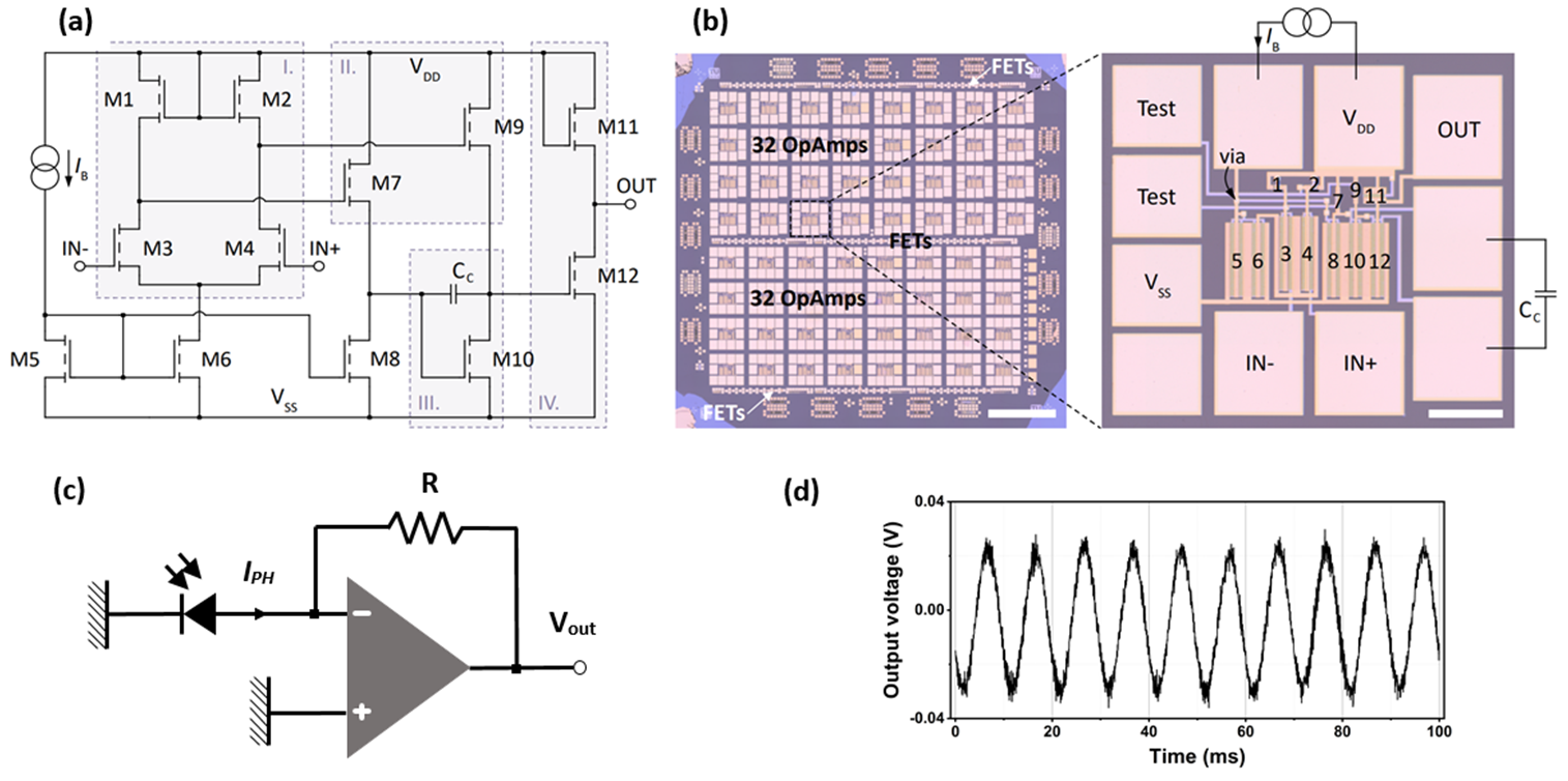
To reduce the device-to-device variability, we took extra care in fabrication process and thanks to the uniform CVD grown MoS2 film managed to achieve excellent performance of the single transistors with small hysteresis, ON/OFF ratios exceeding 8 orders of magnitude and mobility up to almost 20 cm2/Vs. The assessment of more than 40 devices showed a good reproducibility with small variations of the threshold voltage and the charge carrier mobility. Such performance allowed us to combine the transistors into a 4-stage amplifier with total gain of 43 dB in good agreement with the modelling. Moreover, the opamp also showed a good high frequency operation with unity-gain frequency of 0.3 MHz.

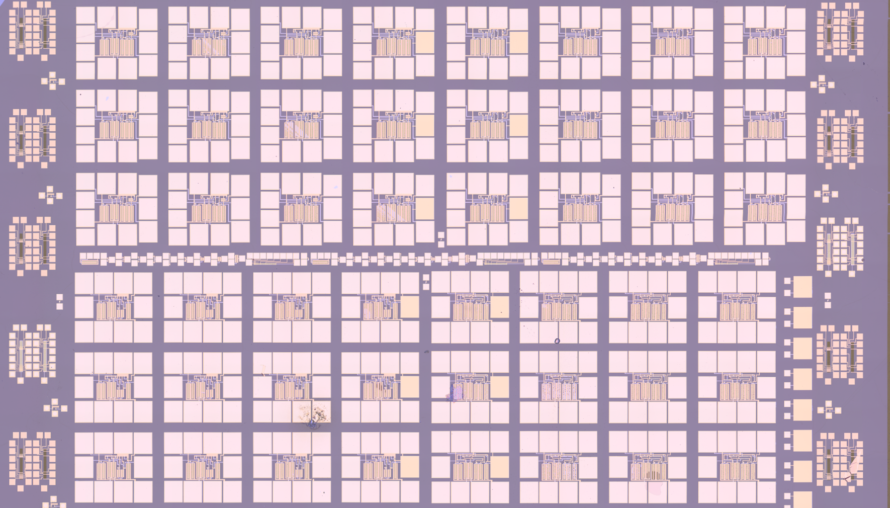
Figure 2. a) Opamp circuit. b) Optical micrograph of the chip, consisting of 64 opamps and test transistors. c) Sketch of the photodetection circuit. d) Output voltage signal from the detection circuit with illumination by incandescent lamp.
To demonstrate the performance of the amplifier we built several feedback circuits commonly employed in electronics - inverting amplifier, integrator, logarithmic amplifier, and transimpedance amplifier. One of the applied applications we used opamp for is the transimpedance amplifier that converts the current of an illuminated photodiode to an output voltage. The results nicely show the characteristic 100 Hz blinking of the classic incandescent bulb used as a light source in the measurement. These experiments demonstrate that 2D opamp can be used in a plethora of applications already in this very prototypical stage. Our work demonstrates that despite an optimisation work is required to improve the parameters of the opamp, manufacturing of such devices on an industrial scale seems possible.
If you are interested in more details of our work, please refer to the paper published in Nature Electronics: “Analogue two-dimensional semiconductor electronics” following the link: https://www.nature.com/articles/s41928-020-0460-6
Follow the Topic
-
Nature Electronics
This journal publishes both fundamental and applied research across all areas of electronics, from the study of novel phenomena and devices, to the design, construction and wider application of electronic circuits.


Please sign in or register for FREE
If you are a registered user on Research Communities by Springer Nature, please sign in
This is a fantastic work because it really addresses the problem of 2D solid-state microelectronic devices and circuits, which is integration and device-to-device variability. Congratulations to all the authors.
Thank you Mario for your comment and congratulations!