Anomalous photovoltaics in Janus MoSSe monolayers

Unlike in p-n junction architectures, the anomalous photovoltaic effect (APE) emerges within asymmetric single-phase materials where photoexcited electron-hole pairs undergo separation driven by spontaneous polarization. The APE is therefore highly desirable for achieving high photovoltaic conversion efficiency to surpass the Shockley–Queisser limit. Two-dimensional (2D) van der Waals (vdW) materials provide a unique opportunity to artificially design symmetries at the interfaces or surfaces for APE. Recently, numerous efforts have been devoted to producing pronounced APE by interfacial engineering with rationally designed stacking, such as MoS2 multilayer homostructure and WS2/black phosphorus heterostructure, etc. Nevertheless, those manipulations are extrinsically localized to the interface between the layers, necessitating the incorporation of a multilayered structure and meticulous control over the interlayer stacking order sustained by the weak vdW interactions.
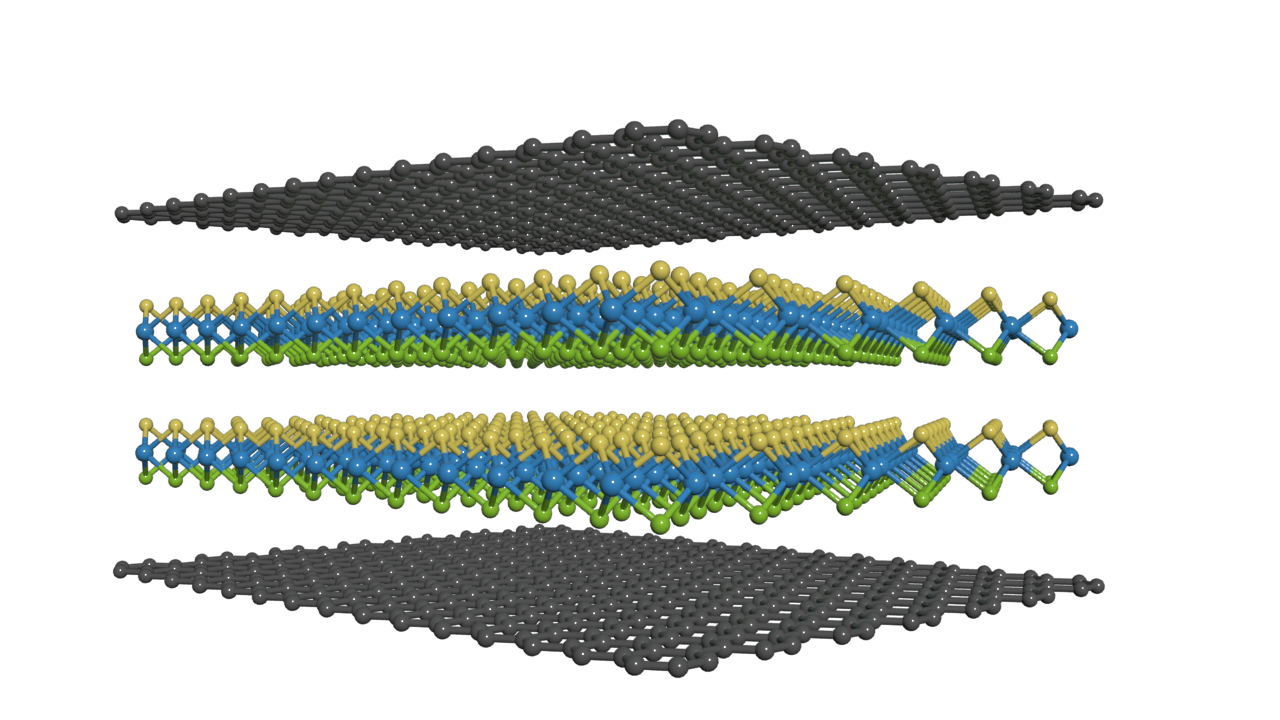
An alternative approach involves atomic manufacturing of the surfaces of the 2D materials for symmetry breaking in a unit material. By using precise composition engineering through selective atom replacement on one side of the 2D TMDs, a Janus monolayer structure with an asymmetric atomic lattice can be synthesized, such as MoSSe. The presence of spatially distinct atoms, sulfur (S) and selenium (Se), results in the breaking of the mirror symmetry and inversion symmetry, leading to pronounced intrinsic out-of-plane polarization (Fig. 1a). The substantial inherent polarity in this system should produce an APE with efficient optoelectronic conversion.
In the recently published work, giant APE in the Janus MoSSe monolayers was demonstrated by the research team led by Prof. Enge Wang, Prof. Kaihui Liu, Dr. Hao Hong and Dr. Chang Liu at Peking University in China. The ultrathin thickness of the polar structure (~0.67 nm thick) facilitates effective photocarrier separation and enhances the APE. An ultrahigh photoresponsivity (up to 3 mA/W, with ~1% external quantum efficiency) was observed in the MoSSe device (Fig. 1b-d). Moreover, the photovoltage can be further scaled up by simply stacking the MoSSe layers without the need for specific control on interlayer twist angles (Fig. 1e). The out-of-plane polarization aligns in the same direction, and the stacking does not diminish the polarization of the crystal. Remarkably, in the MoSSe monolayer device, a significant spontaneous photocurrent (~125 nA) is generated with an open-circuit photovoltage of approximately 0.3 mV. For the three-layer MoSSe device, the photovoltage increases to nearly 0.9 mV and the photocurrent is almost unchanged.
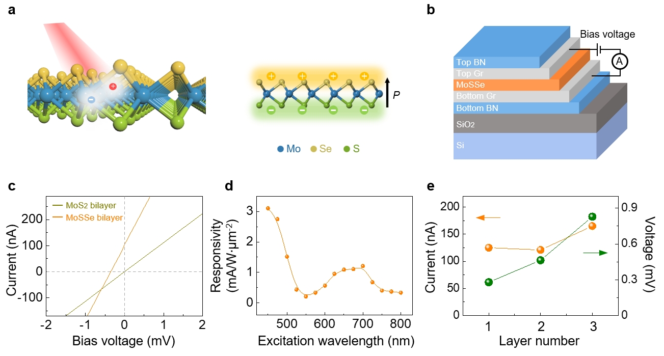
Fig. 1︱Polar structure of the Janus MoSSe monolayer and spontaneous photovoltaic effect in the MoSSe devices. a, Structure of the Janus MoSSe monolayer and the generation of the electron-hole pairs (circles with + and - signs) under optical illumination (left). b, Schematic of the photovoltaic device. c, Short-circuit photocurrent of the MoSSe bilayer and MoS2 bilayer devices as a function of bias voltage under the same illumination conditions. The nonzero photocurrent at zero bias voltage indicates spontaneous photovoltaic responses in the MoSSe device. d, Excitation wavelength-dependent photocurrent responsivity. This peak corresponds to the exciton resonance of MoSSe. e, Layer dependence of the short-circuit current and open-circuit voltage in the MoSSe device. With increasing layer number, the photocurrent remains nearly unchanged, while the voltage increases accordingly.
As for the response time, the ultrathin thickness promises the upper limit speed of the device’s photoresponse. Photocarriers can transfer ultrafast and sufficiently to graphene, avoiding a long out-of-plane drift distance to the electrodes as in bulk materials. Moreover, high-quality interface and strong interfacial coupling are obtained due to the self-passivated surfaces free of dangling bonds. Here in the work, the MoSSe-based device has the intrinsic response time of ~50 ps, corresponding to an intrinsic bandwidth of ~11 GHz, extracted from the ultrafast time-resolved photocurrent autocorrelation spectroscopy. The noise level of the device was obtained to be ~10−21 A2 Hz−1 with zero bias voltage at room temperature. When operating at high frequency, the noise level can be substantially suppressed. Therefore, the MoSSe-based devices show the advantage at high frequency with the intrinsic ultrafast photoresponse.
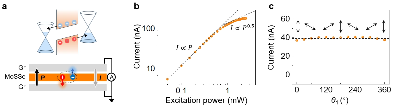
Fig. 2︱Depolarization field-dominated photocurrent generation in the MoSSe devices. a, Schematic of the band alignment (top) and the photocarrier transfer process (both electron and holes) in the device (bottom). The existing depolarization field drives the photocarriers to the interface and leads to a photocurrent (grey arrow) in the direction opposite to the polarization direction (black arrow). b, Excitation power-dependent spontaneous photocurrent. The logarithmic coordinates are used in the figure representation. The dots are the experimental data and the dashed line corresponds to a linear fit. c, Linear polarization direction dependence of the photocurrent by varying the angle ( ) of the waveplates. The horizontal dashed lines are used for eye guidance.
For polar materials with broken inversion symmetry, three APE mechanisms, shift current, injection current and the depolarization field, co-exist for photon harvesting. Given the power-dependent and polarization-dependent photocurrent results (Fig. 2b-c), it’s indicated that the dominant mechanism is the depolarization field in the MoSSe devices. In the depolarization field scenario, the intrinsic out-of-plane polarization ( ) existing in MoSSe induces surface charges with opposite signs in the top and bottom graphene electrodes. The electrons in the electrodes can screen the surface charges, and two dipoles with the same direction form at the two electrode‒sample interfaces. Each dipole is responsible for an electrostatic potential drop ( ) in the same direction. Since the induced charges cannot fully compensate for the polarization charges in MoSSe, the resulting depolarization field inside the material drives the separation of the electron–hole pairs, which can be collected by the graphene electrodes via interfacial charge transfer, thus forming a spontaneous photocurrent (Fig. 2a). Remarkably, the depolarization field established is inversely proportional to the film thickness. A thinner polar film will lead to a stronger depolarization field and more efficient APE. The magnitude of the depolarization field in the MoSSe device can be estimated by the band diagram and related open circuit voltage, which gives the upper bound value on the order of ~104 kV/cm.
Compared with other photovoltaic materials, Janus MoSSe has numerous figures of merit. The polarization state of MoSSe originates from the intrinsic asymmetric atomic lattice that can stably exist at the thickness of ~0.67 nm. It’s expected to be the thinnest photovoltaic devices with giant photocurrent responsivity within the entire family of 2D material. Moreover, the enhanced depolarization field and the reduced diffusion length of photocarriers increase the efficiency. On the other hand, MoSSe-based devices are also limited by the typical disadvantages such as lack of polarization switching, existence of strain and extrinsic contamination, and the challenge of mass production. Overall, Janus TMDs are promising candidates to facilitate the development of miniaturized, high-integrated, and flexible thin-film optoelectronic and photovoltaic devices.
Follow the Topic
-
Nature Communications
An open access, multidisciplinary journal dedicated to publishing high-quality research in all areas of the biological, health, physical, chemical and Earth sciences.

Related Collections
With Collections, you can get published faster and increase your visibility.
Women's Health
Publishing Model: Hybrid
Deadline: Ongoing
Biosensing
Publishing Model: Hybrid
Deadline: Sep 30, 2026


Please sign in or register for FREE
If you are a registered user on Research Communities by Springer Nature, please sign in