Beyond the Silicon Plateau: A Convergence of Novel Materials for Transistor Evolution
Published in Materials

As Moore’s law approaches its physical limits, the semiconductor industry faces mounting challenges in power efficiency, leakage control, and device reliability. Now, researchers from Seoul National University, Kookmin University, Northwestern University, and Texas A&M, led by Professor Ho Won Jang and Professor Yoon Jung Lee, have published a comprehensive review exploring next-generation transistor materials and architectures. This work provides a roadmap for overcoming the limitations of traditional silicon-based devices through innovative material systems and device integration strategies.
Why Novel Transistor Materials Matter
- Scaling Bottlenecks: Silicon transistors are struggling with short-channel effects, high leakage, and power density issues at sub-10 nm nodes.
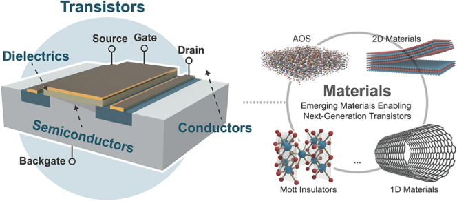
- Energy Efficiency: New materials like 2D semiconductors, Mott insulators, and halide perovskites offer ultra-low power switching and high carrier mobility.
- 3D Integration: Advanced materials enable monolithic 3D stacking and heterogeneous integration, extending Moore’s law beyond planar scaling.
- AI Hardware Compatibility: Emerging materials support neuromorphic computing, in-memory processing, and adaptive learning systems.
Innovative Design and Features
- 2D van der Waals Semiconductors: Atomically thin channels (e.g., MoS2, InSe, WSe2) provide pristine interfaces, reduced scattering, and excellent gate control.
- Mott Insulators: Materials like VO2 enable abrupt metal-insulator transitions for steep-slope switching (<10 mV/dec).
- Halide Perovskites: Defect-tolerant, solution-processable semiconductors with ambipolar transport and neuromorphic functionalities.
- Amorphous Oxide Semiconductors (AOS): High mobility, low-temperature processability, and scalability for flexible and transparent electronics.
- Advanced Dielectrics: High-K, ferroelectric, and 2D dielectrics (e.g., HfO2, hBN) enhance gate control and reduce leakage.
- Topological Interconnects: Weyl semimetals and 2D metals offer scattering-free, low-resistance pathways for back-end-of-line integration.
Applications and Future Outlook
- Sub-60 mV/dec Switching: TFETs, NC-FETs, and DSFETs leveraging 2D materials and ferroelectrics to break the thermal limit.
- Neuromorphic Devices: Perovskite and Mott-based transistors emulate synaptic plasticity for brain-inspired computing.
- 3D Monolithic Integration: Vertical stacking of logic and memory layers using low-temperature, CMOS-compatible processes.
- Thermal Management: Embedded microfluidic cooling, high-K heat spreaders, and AI-driven thermal regulation for 3D chips.
- Sustainable Manufacturing: Green processing, recyclable materials, and energy-efficient fabrication for eco-friendly electronics.
Challenges and Opportunities
The review emphasizes the need for interface engineering, material stability, and CMOS compatibility. Future research will focus on co-optimizing materials, device structures, and system-level integration to realize ultra-scaled, energy-efficient, and intelligent transistor technologies.
This comprehensive review charts a transformative path beyond silicon, highlighting the convergence of novel materials, 3D architectures, and AI-driven design. It underscores the importance of cross-disciplinary innovation in shaping the future of electronics. Stay tuned for more groundbreaking work from Professor Ho Won Jang and Professor Yoon Jung Lee’s teams!
Editor of Nano-Micro Letters, which is an Open-Access, peer-reviewed journal reported papers that have at least one dimension ranging from a few sub-nanometers to a few hundreds of micrometers. The journal is published by Springer Nature and indexed by SCI, EI, SCOPUS, Pubmed, etc. The 2024 JCR Impact Factor is 36.3. The 2024 CiteScore is 53.1.
Follow the Topic
-
Nano-Micro Letters

Nano-Micro Letters is a peer-reviewed, international, interdisciplinary and open-access journal that focus on science, experiments, engineering, technologies and applications of nano- or microscale structure and system in physics, chemistry, biology, material science, and pharmacy.


Please sign in or register for FREE
If you are a registered user on Research Communities by Springer Nature, please sign in