Coulomb blockade in an atomically thin quantum dot coupled to a tunable Fermi reservoir
Published in Electrical & Electronic Engineering
Could you briefly outline the key findings of your paper?
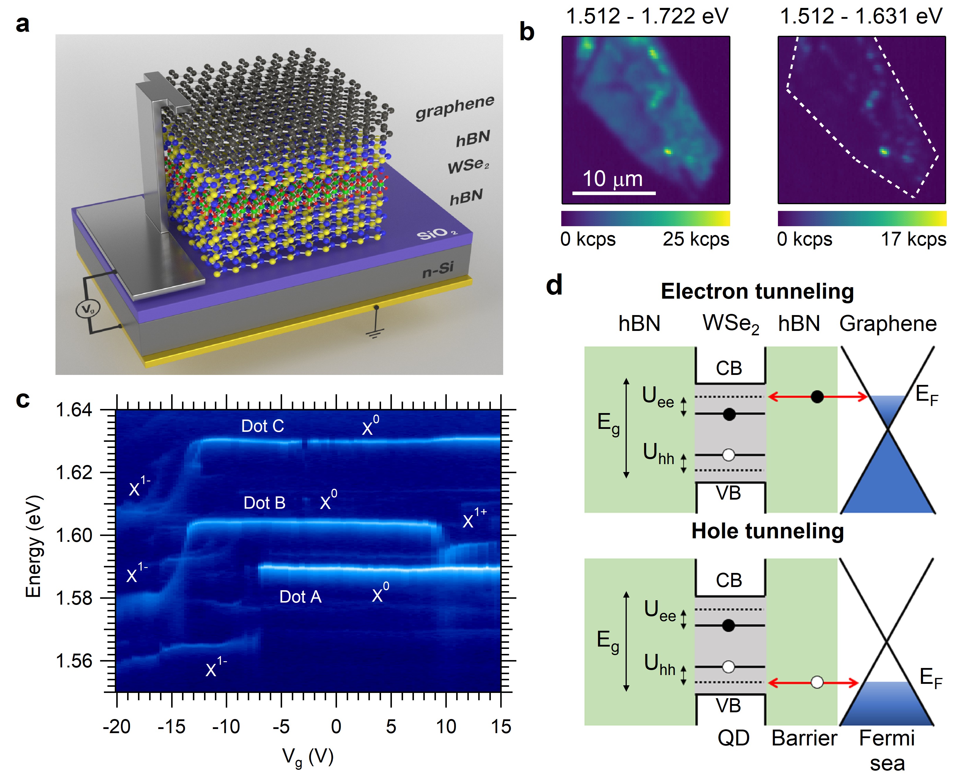
We have achieved the deterministic loading of individual particles (such as an electron or a hole – which is an absence of an electron so has the opposite charge) in a two-dimensional semiconductor quantum device. “Two-dimensional” means the device is made by precisely stacking different layers of materials which are just one atom thick. “Quantum” means we can trap particles to a region (made of a WSe2 crystal) so small that it collectively behaves like a single (artificial) atom which exhibits all the hallmarks expected from quantum mechanics; when an electron and a hole are trapped, they can combine to create a photon – a single particle of light. “Device” means that, simply applying an electrical voltage, we can load the particles one-by-one.
The loading of individual particles in these atomically thin quantum dots was possible due to quantum tunnelling, a quantum mechanical phenomenon whereby subatomic particles can pass through a potential barrier (like a wall)- something not possible in our everyday non-quantum world. According to quantum mechanics, when the quantum tunnelling is highly likely, the particle’s position can be described by a probability that it is located on both sides of the wall. In our device, the ‘wall’ was a single sheet of atoms, so the probability that it could be on both sides was very high, and we were able to tune this simply by changing a voltage to a device. This led to dramatic effects when the light was emitted from the quantum dot.
What is your role in this work?
This work is the result of an international research collaboration led by the Quantum Photonics Lab at Heriot-Watt University. Researchers from the National Institute for Materials Science in Japan provided high quality crystals of hexagonal Boron Nitride – these formed the tunnel barrier or ‘wall’ for the single particles. The assembly of the 2D semiconductor heterostructure was carried out with the collaboration of researchers from the Boston College Department of Physics in the United States, who have an ultra-pure environment to assemble the atomic layers. Finally, I did the characterization of the device and the subsequent data analysis and interpretation with colleagues from the Quantum Photonics Laboratory, led by Prof. Gerardot.
What was the genesis of this paper? How did you come to this particular problem?
In 2015, several research groups demonstrated that a single layer of WSe2 can host quantum dots light emitters. These single photon sources in a single sheet of atoms offer new opportunities for integrated and scalable quantum photonic chips for applications in quantum information science. Simultaneously, several groups were trying to figure out how to load particles into quantum dots made by placing metallic gates around a 2D semiconductor, with the motivation that the properties of the single electrons or holes could be engineered and understood. We were able to successfully combine these two ideas and apply device concepts that have been developed in bulk (3D) semiconductors over the last 15 or 20 years or so to this new field of atomically thin semiconductors.
What is the most empowering implication of your results?
The 2D material platform offers exciting opportunities to combine different types of atomic sheets (insulators, semiconductors, magnetic materials, etc), giving us access to unique physics that wasn’t possible with conventional bulk semiconductors. Our results show that we can make such devices at the quantum level – controlling a single trapped particle in a deterministic way. This will enable us to better understand the quantum properties of 2D materials and enable new types of experiments, in particular where the particles which are tunnel coupled to the quantum device can have interesting properties, for instance from a magnetic material or graphene. Ultimately this could lead to new technologies based on quantum mechanics.
How have 2D materials been uniquely instrumental to enabling these results?
There are a few unique aspects of our results compared to what has previously been done with conventional semiconductors. The first is that the tunnel barrier is atomically thin – this means the quantum mechanical tunnelling is much stronger than what has been achieved before. Secondly, the quantum dots in WSe2 are quite unique compared to conventional quantum dots: they have very large inter-particle interactions (called Coulomb interactions) that led to our observation of new features for the strong tunnel coupling regime – for instance how different energy states couple to the sea of particles in the electrode. Finally, because we used few layer graphene for the electrode, we were able to choose either electrons or holes to load into the QD. This isn’t possible with a conventional metal.
Can you describe the main challenges associated to the preparation of this manuscript? Any anecdotes you’d like to share with us?
Main challenges of the work: the need of ultraclean interfaces in the stacking of different layers of materials one atom thick. Probably the most surprising result is how well the device works, demonstrating that the interfaces between the different sheets of atoms are truly pristine with no contamination or moisture. This is somewhat remarkable as making it involves the ‘scotch tape’ method (although special polymers rather than tape are used). Compared to how traditional semiconductors are ‘grown’ in an ultra-high vacuum, it is quite crude. Nevertheless, the functionality and strong tunnel coupling observed demonstrates how clean the process can be.
In fact, we had made other devices which showed a bit of evidence of loading a single particle into the quantum dot, but the experimental signatures were not very clean. We think the interfaces in these devices were not pristine enough. But, when we started to measure the current device we saw the dramatic effect of the tunnelling on the colour of light emitting from the quantum dots: we could smoothly adjust the probability for the particle to be in the quantum dot or not, creating something we call a “hybrid exciton”. This was a “eureka” moment for us and quite exciting! We were then able to apply a fairly simple quantum mechanical model to explain the data, and the model fit spectacularly well, confirming our interpretation.
And now, what’s next?
We plan to make new devices where the tunnel coupling is either in the strong or weak tunnel coupling regime.
In the weak coupling regime, the particle in the quantum dot is very well isolated from the sea of particles in the electrode – which means it is a very quiet environment to investigate and manipulate its quantum properties.
In the strong coupling regime, we’d like to investigate the collective behaviour of the isolated particle with the sea of particles. In particular, we’d like to examine this collective behaviour with the sea of particles in graphene. It should lead to interesting many-body interactions first described by a physicist named Kondo.
Finally, we’d like to replace the graphene with a 2D ferromagnet, so that we can take control of the magnetic properties of the particles. This could lead to a ‘spintronic’ quantum device.
The related paper has been published in Nature Nanotechnology. Please see details:
Mauro Brotons-Gisbert, Artur Branny, Santosh Kumar, Raphaël Picard, Raphaël Proux, Mason Gray, Kenneth S. Burch, Kenji Watanabe, Takashi Taniguchi and Brian D. Gerardot, "Coulomb blockade in an atomically thin quantum dot coupled to a tunable Fermi reservoir", Nat. Nanotechnol. DOI: 10.1038/s41565-019-0402-5
Follow the Topic
-
Nature Nanotechnology
An interdisciplinary journal that publishes papers of the highest quality and significance in all areas of nanoscience and nanotechnology.


Please sign in or register for FREE
If you are a registered user on Research Communities by Springer Nature, please sign in