Face-centered cubic carbon as a fourth basic carbon allotrope with properties of intrinsic semiconductors and ultra-wide bandgap
Published in Materials

Thin films of face-centered cubic carbon (fcc), which we designated as 'quasivalent carbon' were obtained by plasma-assisted chemical vapour deposition (PACVD) from CH4-H2 gas mixtures on single-crystalline diamond substrates by use of very peculiar deposition conditions.
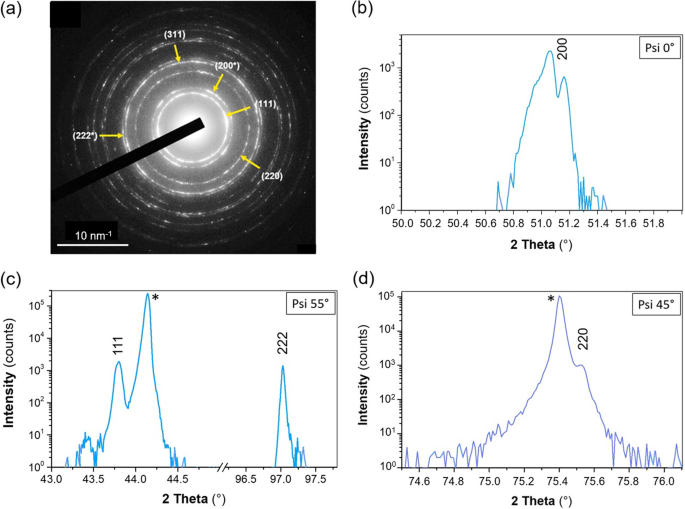
An electron diffraction pattern obtained from nano-sized fregments of the film detached from the film surface by a copper grid, showed in Table 1, indicates a typical pattern of the face-centered cubic carbon. Table 1 also shows several XRD peaks from the film. Results of electron diffraction and X-ray diffraction presented in Table 1 clearly indicate that quasivalent carbon has a face-centred cubic crystal lattice with the space group Fm-3m.The high-resolution TEM (HRTEM) image from the film confirms the mentioned above.
How can the existence of quasivalent carbon be explained theoretically when taking into account that carbon has only 4 valent electrons but the face-centered cubic crystal lattice is characterised by the coordination number of 12?
To answer this question ab initio calculations of the electronic structure of quasivalent carbon were conducted.
The valence band of quasivalent carbon was found to be separated from the conduction band by a large band gap (about 7.1 eV), which is consistent with the value established experimentally. However, the Fermi level falls on the top of the valence band, which is half-filled. For this reason, despite the large band gap, quasivalent carbon is expected to have properties of an intrinsic semiconductor. We found that the valence states closest to the Fermi level generate an insignificant density of delocalized electrons between carbon atoms allowing the mobility of electrons throughout the whole crystal lattice, which results in its electrical conductivity.
Unlike diamond, the valence band of quasivalent carbon is split into a lower and an upper part by an intraband gap of about 0.8 eV. Therefore, it can be expected that in spectra from quasivalent carbon obtained by different methods, such as XPS, there should be two peaks, the separation of which is expected to be about 0.8 eV. Indeed, splitting of the core C1s peak in the X-ray photoelectron spectrum obtained from quasivalent carbon into two peaks separated by nearly 0.6 eV was observed experimentally. This is supposed to indicate that the 3 p-electrons in the electronic structure are nearly hybridized, whereas the rate of hybridization of s- and p-electrons appears to be very insignificant. The theoretically established very low degree of hybridization of s and p electrons leads to the phenomenon that the three p electrons in the configuration 2s12p3 form a 3D symmetrical electronic cloud. Each electronic cloud can therefore overlap with the electronic clouds of 12 neighboring carbon atoms thus forming the Fm-3m fcc crystal lattice with the coordination number of 12.
An X-ray photoelectron spectrum from the quasivalent carbon film comprises the C1s signal split into two peaks at 283.8 eV and 284.4 eV as well as signals typical for C-O bonds due to oxygen adsorbed on the film surface. The split was predicted by the ab initio calculations mentioned above and indicates the presence of nearly unhybridized s and p electrons in the electronic structure of quasivalent carbon.
The Raman spectrum recorded from a small fragment detached from the film by a Cu grid does not comprise any signals, which was confirmed by conducting Raman spectroscopy from a number the carbon agglomerated particles located in different cells of the Cu grid. It is well known that materials with a face-centered cubic crystal lattice (the primitive unit cell of which contains only a single atom) have only acoustic phonons and no optical phonons. In Raman spectra, only optical phonons are observed; acoustic phonons have practically zero frequencies in the long-wavelength limit of the spectra, so such materials do not show signals in their Raman spectra, which explains the Raman spectra from quasivalent carbon.
The electrical conductivity of quasivalent carbon at room temperature is relatively high and comparable with that of conventional intrinsic semiconductors despite the wide band gap. The temperature dependence of conductivity provides clear evidence that the nature of electrical conductivity in quasivalent carbon is similar to that in semiconductors.
It can be assumed that quasivalent carbon represents a new class of inorganic solids characterized by conductivity due to noncovalent sharing p-electrons, which leads to the presence of some delocalized electrons only in the regions of overlapping electronic clouds of carbon atoms thus ensuring the mobility of electrons throughout the whole crystal lattice.
The combination of different apparently contradictory properties makes quasivalent carbon an ideal candidate for numerous applications as a transparent semiconductive material in a wide range of technologies, including fabrication of thin-film transistors, transparent electronics, flat screen displays and photovoltaics, etc. as well as novel and unexpected applications in the field of ‘carbon electronics’.
Table 1
Spacing d and indexing hkl of diffractions patterns of metametallic carbon according to refs.5,6 and the present work.
|
hkl |
dexp. (Å) for quasivalent carbon with the fcc crystal lattice according to literature. |
dcalc. (Å) for quasivalent carbon with the fcc crystal lattice with a0=3.563Å, according to literature. |
d (Å) for quasivalent carbon according to the present work |
|
|
111 |
2.067 |
2.057 |
2.058*/2.076+0.005** |
|
|
200+ |
1.791 |
1.781 |
1.786*/1.787+0.0015** |
|
|
220 |
1.261 |
1.260 |
1.266*/1.257+0.0008** |
|
|
311 |
1.078 |
1.074 |
1.074* |
|
|
222+ |
1.032 |
1.029 |
1.030*/1.0298+0.005** |
|
|
400 |
0.892 |
0.891 |
0.893*/0.891+0.0015** |
|
|
331 |
0.817 |
0.817 |
0.812* |
|
|
420+ |
0.796 |
0.797 |
0.783* |
|
|
422 |
0.727 |
0.727 |
0.720* |
|
|
331/511 |
0.686 |
0.686 |
0.680* |
|
|
440 |
0.630 |
0.630 |
0.630* |
|
|
531 |
0.601 |
0.602 |
0.550* |
* Reflections according to the electron diffraction pattern.
** Reflections obtained based on basis of the XRD results.
+ Reflections forbidden for the diamond crystal lattice
Follow the Topic
-
Communications Materials
A selective open access journal from Nature Portfolio publishing high-quality research, reviews and commentary in all areas of materials science.
Related Collections
With Collections, you can get published faster and increase your visibility.
Materials for quantum sensing and computing
Publishing Model: Open Access
Deadline: Jul 09, 2026
Triboelectric nanogenerators for energy harvesting
Publishing Model: Open Access
Deadline: Jun 30, 2026


Please sign in or register for FREE
If you are a registered user on Research Communities by Springer Nature, please sign in