Face‑/Edge‑Shared 3D Perovskitoid Single Crystals with Suppressed Ion Migration for Stable X‑Ray Detector

As X-ray detection plays an indispensable role in industrial inspection, medical diagnosis, and security checks, the search for high-performance detection materials has never been more critical. Traditional three-dimensional (3D) metal halide perovskites show great promise for direct X-ray detection, yet their inherent ion migration severely undermines detector stability—hindering commercialization. Now, a collaborative team of researchers from institutions including Henan University, Shenzhen Institute of Advanced Technology (Chinese Academy of Sciences), and Shaanxi Normal University has developed a game-changing solution: face-/edge-shared 3D heterometallic glycinate hybrid perovskitoid single crystals (SCs) with suppressed ion migration. Their findings, published in Nano-Micro Letters, offer a new pathway for stable, high-sensitivity X-ray detection.
Why These 3D Perovskitoid SCs Stand Out
The core innovation lies in the unique design of the perovskitoid crystals, which addresses the long-standing ion migration issue of traditional perovskites while preserving key detection capabilities:
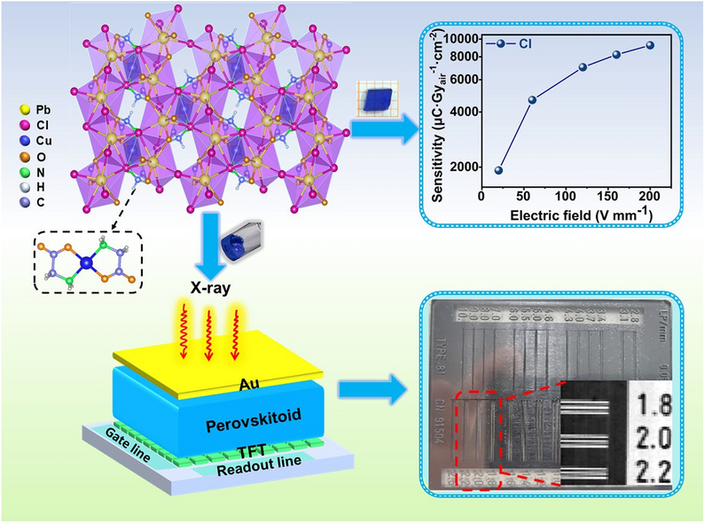
- Synergistic Ion Migration Suppression: The crystals (formula: Pb2CuGly2X4, where Gly=−O2C−CH2−NH2 and X=Cl/Br) feature a robust structure: large-sized Cu(Gly)2 pillars link adjacent lead halide layers, while a face-/edge-shared inorganic skeleton (composed of [PbX5O3]9− dodecahedrons) adds rigidity. Together, these components boost the ion migration activation energy (Ea) to 1.06 eV for the Cl-based variant—far higher than that of conventional 3D perovskites—effectively curbing ion movement.
- Ultra-Low Dark Current Drift: Under harsh conditions (120 V mm−1 electric field and 2.86 Gy continuous X-ray irradiation), the Pb2CuGly2Cl4 SC detector exhibits an extremely low dark current drift of 1.20×10⁻⁹ nA mm−1 s−1 V−1. This stability ensures consistent response signals, a critical requirement for long-term operation.
- High Sensitivity & Detection Efficiency: The Pb2CuGly2Cl4 SC detector delivers a sensitivity of 9250 μC Gy−1cm−2—over 21 times higher than commercial α-Se detectors (which require a much stronger electric field of 15,000 V mm−1). Its detection efficiency for 50 keV X-rays reaches 145%, outperforming the Br-based counterpart (∼124%).
Key Design, Synthesis, and Performance Details
1. Crystal Structure & Synthesis
The team synthesized high-quality Pb2CuGly2X4 SCs via a simple water evaporation method:
-
- Precursor solutions (containing PbX2, CuX2, and glycine) were stirred at 100 °C, then rapidly evaporated to form seed crystals.
- Slow evaporation of supersaturated solutions (50 °C for 14 days) yielded large-sized SCs: Pb2CuGly2Br4 (dark blue, ~4 mm × 3 mm × 1.2 mm) and Pb2CuGly2Cl4 (light blue, ~3 mm × 2 mm × 0.7 mm).
- XRD analysis confirmed the crystals’ high crystallinity, with the Cl-based SC showing smaller lattice constants and lower microstrain (0.02 vs. 0.07 for the Br-based SC)—indicating fewer defects and better structural quality.
2. Optoelectronic Advantages
Density functional theory (DFT) calculations and experimental characterizations revealed additional strengths:
-
- Both SCs are direct semiconductors (band gaps: 3.12 eV for Cl, 2.94 eV for Br) with a broad absorption range (visible to near-infrared), enabled by
- transitions of Cu2+.
- The Pb2CuGly2Cl4 SC has a higher resistivity (2.18×10¹² Ω cm) and lower trap density (2.1×1010 cm−3) than its Br-based counterpart. These properties reduce noise and enhance charge collection, as reflected in its higher carrier mobility-lifetime product (μτ=3.65×10⁻⁴ cm2 V−1).
3. Toward Practical Imaging: TFT Array Detector
To enable real-world X-ray imaging, the team developed a scalable thin-film transistor (TFT) array detector:
-
- Pb2CuGly2Cl4 nanocrystals were dispersed in water to form a paste, which was blade-coated onto a 64×64 pixel TFT array (200×200 μm2 per pixel) and annealed at 100 °C.
- The resulting detector achieved a spatial resolution of 2.2 lp mm−1—sufficient to clearly image the internal circuits of a network cable plug. While its sensitivity (4490 μC Gy−1cm−2 at 100 V mm−1) is lower than the SC-based detector (due to film defects), it demonstrates the feasibility of low-cost, large-area imaging devices.
Future Outlook & Significance
This work addresses a core challenge in perovskite-based X-ray detection: balancing sensitivity with stability. The amino acid ligand-metal cross-linking strategy not only expands the library of 3D perovskitoid materials but also provides a general design principle for suppressing ion migration in ionic semiconductors.
Looking ahead, the team aims to optimize the quality of Pb2CuGly2Cl4 thin films to further boost the TFT array detector’s sensitivity. Additionally, exploring other metal-amino acid combinations could unlock even higher-performance materials for next-generation X-ray imaging systems—from medical radiography to industrial non-destructive testing.
Stay tuned for more innovations from this collaborative team, as they continue to bridge materials design and practical detection applications!
Editor of Nano-Micro Letters, which is an Open-Access, peer-reviewed journal reported papers that have at least one dimension ranging from a few sub-nanometers to a few hundreds of micrometers. The journal is published by Springer Nature and indexed by SCI, EI, SCOPUS, Pubmed, etc. The 2025 JCR Impact Factor is 38.5. The 2025 CiteScore is 58.9.
Follow the Topic
-
Nano-Micro Letters
Nano-Micro Letters is a peer-reviewed, international, interdisciplinary and open-access journal that focus on science, experiments, engineering, technologies and applications of nano- or microscale structure and system in physics, chemistry, biology, material science, and pharmacy.


Please sign in or register for FREE
If you are a registered user on Research Communities by Springer Nature, please sign in