Highly Sensitive On-Chip Electromagnetic-To-Optical Signal Conversion Using Nitrogen Vacancy (NV) Diamond-Embedded Nanocoils
Published in Bioengineering & Biotechnology

What’s so special about our coil?
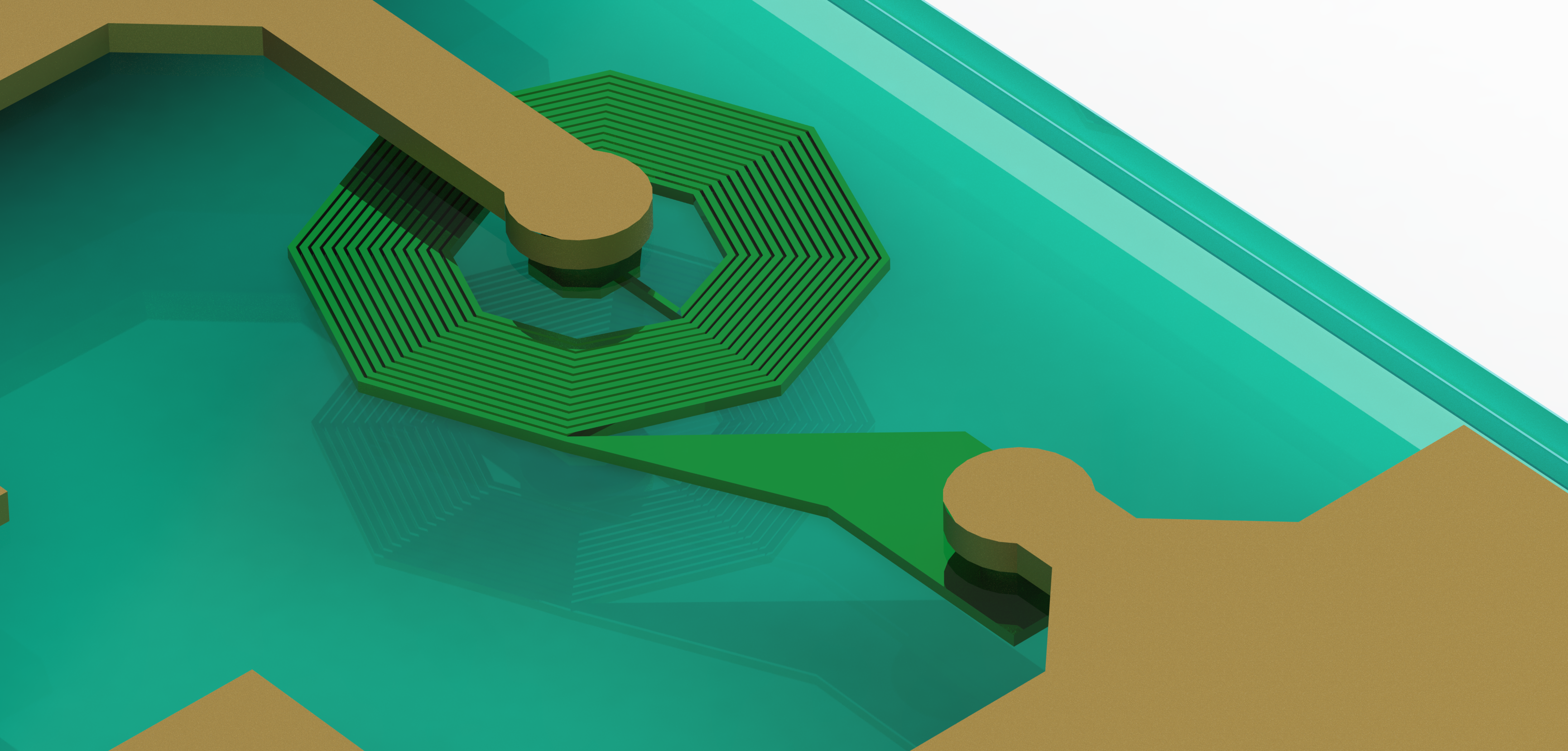
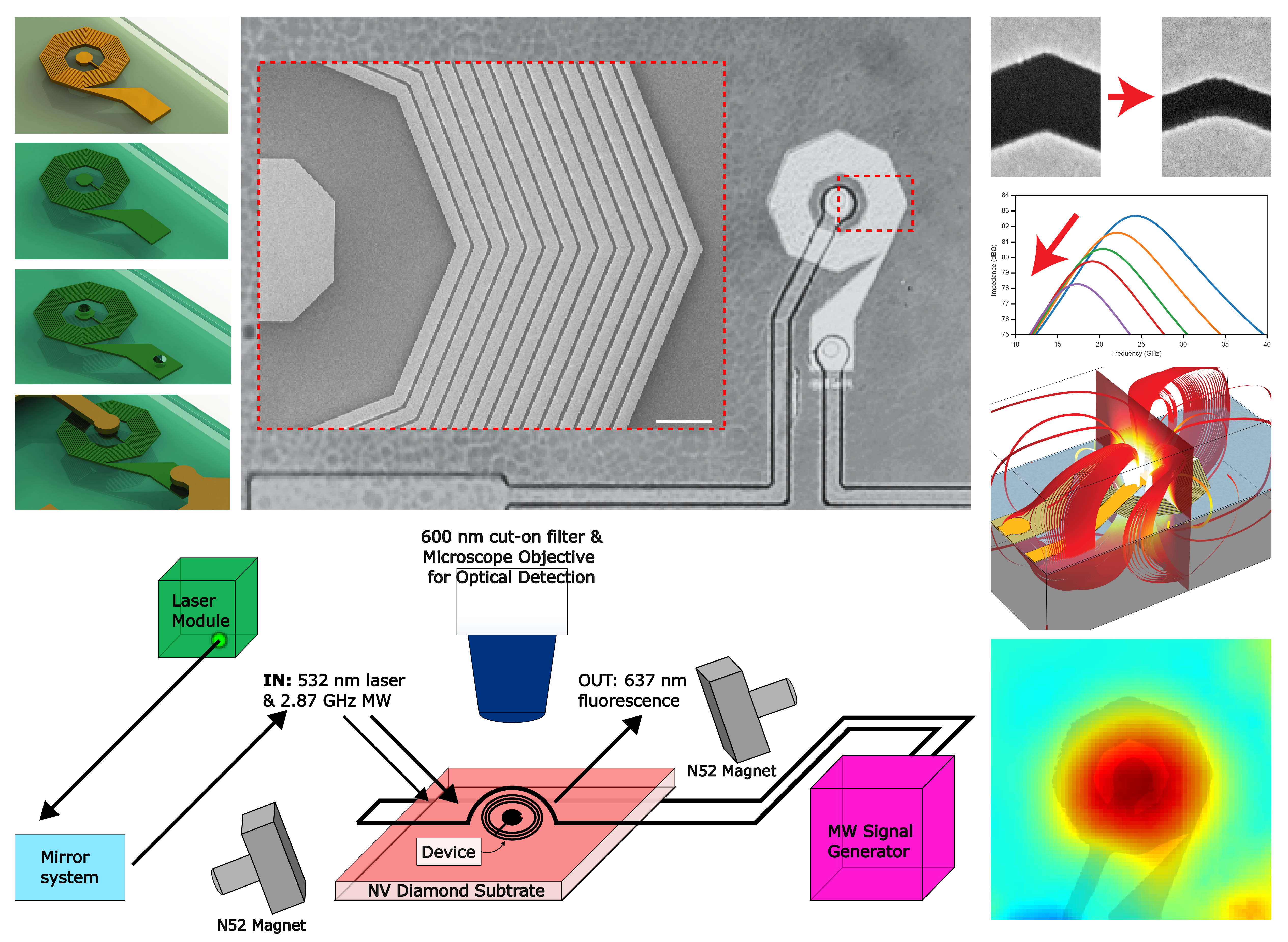
Although a conductive coil doesn’t sound all that intriguing, scientists at the University of Wisconsin-Madison have created a versatile nitrogen vacancy (NV) diamond-embedded nanofabricated coil (nanocoil). This innovation serves as a highly efficient electro-magneto-optical transduction platform, greatly augmenting a variety of biological and environmental detection and stimulation scenarios. While many on-chip coil designs leverage highly involved synthesis, our approach utilized rapid electron-beam lithography to generate coils with dose-dependent tunable electromagnetic properties [1]. We employ optically detected magnetic resonance (ODMR) to obtain sensitive readouts of current-induced magnetic fields and correlate our measurements with numerical methods to validate their suitability for integrated applications. One immediate and exciting avenue for using this technology is to detect minute biogenic magnetic fields with exceptionalspatial resolution and sensitivity [2].
Our methodology and findings
In the paper, we first survey the existing state of the art and explain the nuances behind our results for each analysis we undertake. We intermesh finite element models of device operation with characterization fabrication process parameters. We present resulting topography data of the device using atomic force microscopy and high resolution scanning electron microscopy affirming a linear, dose-dependent turn width and gap spacing trend in agreement with our modeling. We describe how we used these data to determine trends in electromagnetic properties versus dose, paving the way towards tuning these sensors for radiofrequency applications including ODMR, magnetic resonance imaging (MRI) and more. We explain how the amount of power dissipated by the coils increases linearly with the dose used to pattern each coil. Finally, we show how injecting current into coils and imaging them using NV magnetometry reveals homogeneous field profiles within the sensitive area. A schematic of our optical setup is shown in detail in the bottom panel of the graphical abstract included here. The use of NV diamond substrate allows for high sensitivity magnetometry in ambient conditions at high spatial resolution. While other magnetometry techniques may require supercooled helium to generate zero field conditions, NV magnetometry can operate at room temperature conditions relying on simple small-field permanent magnets to generate sufficient bias fields.
Technological impact and future applications
Our work establishes NV magnetometry more broadly for the measurement and validation of micro- and nano-scale on-chip probes. NV centers in diamond can be utilized in vector magnetometry to optically measure the fields generated by probes in parallel. By orienting the bias field so that all four NV axes have a different component of the field along them, a user can easily discern four distinct photonic splits in the spectral response corresponding to these axes. By analyzing these splits, a 3D field map can show not only field magnitude generated by probes, but field direction as well. Embedding nanofabricated coils within nitrogen-vacancy diamond substrate provides a highly customizable platform for tuning turn width and turn spacing by carefully controlling electron beam to operate and greatly augment optically detected magnetic resonance for visualizing magnetic fields at high resolution. Our technology lays the foundation for broadly applicable on-chip electromagneto-optical sensing and modulation and establishes a highly reproducible and rapid synthesis easily accessible toother groups.
The team
Central to the project was Ilhan Bok’s work establishing finite element models and analyzing data acquired through the nanofabrication and nanoscale imaging travails of Dr. Alireza Ashtiani and magnetometry performed by Yash Gokhale, M.S. using custom-built magnetometry apparatus. Dr. Jack Phillips and Tianxiang Zhu, M.S. contributed to modeling and instrumentation, respectively, and all authors worked under the supervision of principal investigator Dr. Aviad Hai. Our work appears in the journal Microsystems & Nanoengineering [1], where we provide increased insight into our device and further quantify the results obtained from our simulations and experiments.
Follow the Topic
-
Microsystems & Nanoengineering
This journal, with a target for a high-end journal for years to come, seeks to promote research on all aspects of microsystems and nanoengineering from fundamental to applied research.


Please sign in or register for FREE
If you are a registered user on Research Communities by Springer Nature, please sign in