InGaAs high-speed detector directly coupled to SOI waveguide
Published in Electrical & Electronic Engineering
As the amount of data generated from modern communication applications is increasing rapidly, silicon electronic integrated circuits (ICs) are suffering from a bottleneck at the interconnection level. The best way to overcome this obstacle is to combine electronics and photonics on a silicon chip and get the best of both computation and transmission.
Electrons are ideal for computation because they allow for ultimately scaled logic gates which can be integrated in a massively parallel fashion using modern CMOS technologies. Photons on the other hand are ideal for transmission because this can be done almost loss-less on chip-size length scales. Whereas state-of-the-art high-speed detectors today are based on germanium, III-V materials with direct bandgap and the opportunity for lattice-matched heterojunctions are needed for efficient light emission. Thus, to enable a fully integrated optical link, there is a need to integrate alternative materials such as III-Vs on a silicon chip.
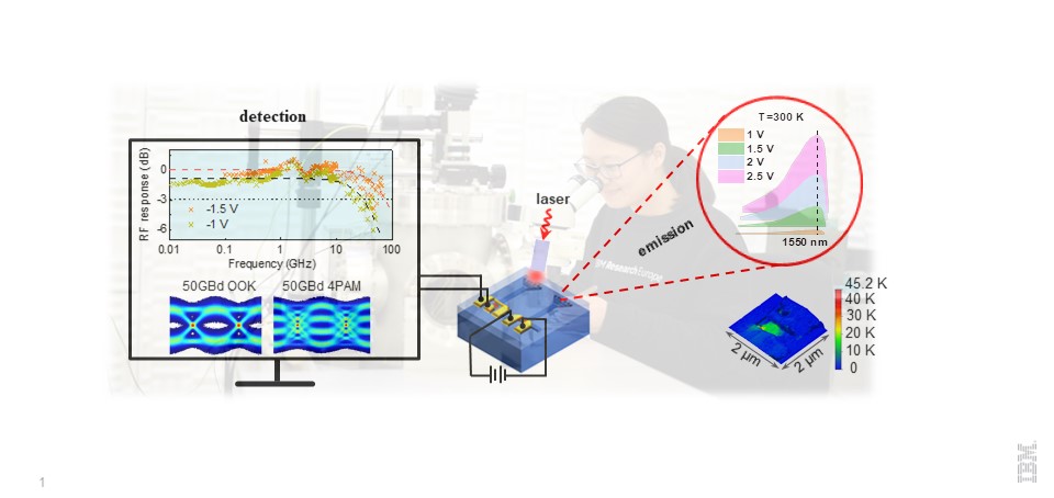
The seamless integration of III-V nanostructures on silicon is a long-standing goal and an important step towards integrated optical links. In this work, which is a joint collaboration between IBM Research Europe – Zurich and the ETHZ, we demonstrate fully waveguide coupled III-V photodetectors monolithically integrated on silicon. In addition to realizing a waveguide coupled scheme and scaling the detectors, we also implement a double heterostructure (n-InP/i-InGaAs/p-InP) to improve carrier confinement compared to earlier work. Presently, a cutoff frequency f3dB, exceeding 70 GHz was achieved for photodetection in reverse bias. Using grating couplers centered around 1320 nm, we evaluate the detector performance under various signal encoding schemes and successfully demonstrate data reception at 50 GBd with OOK and 4PAM. While operating the p-i-n diodes in forward bias regime, light emission in LED mode centered at 1550 nm was observed.
Furthermore, thermal effects are detrimental to device performance and reliability in scaled photonic devices. In this work, we investigate the in-situ temperature increase by scanning thermal microscopy (SThM) and compare the results with thermal simulation by Ansys, establishing that the associated temperature increase during device operation is within the acceptable range.
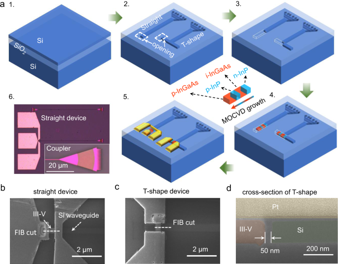
This work demonstrates the first steps towards a full III-V based active photonic link monolithically integrated on silicon-on-insulator (SOI). The presented in-plane integration of the III-V heterostructure p-i-n diode self-aligned to a Si waveguide represents a new paradigm for mass production of densely integrated hybrid III-V/Si photonics schemes. By using the same approach for the integration of the detector and the emitter and an integration technique which enables heterojunctions along the growth direction, this can also be extended to an all-optical high-speed link on Si in the future without the need for evanescent coupling.
This work was partially funded by the European Union H2020 ERC Starting Grant project PLASMIC (Grant Agreement #678567) and H2020 MSCA IF project DATENE (Grant Agreement #844541).
Follow the Topic
-
Nature Communications
An open access, multidisciplinary journal dedicated to publishing high-quality research in all areas of the biological, health, physical, chemical and Earth sciences.

Related Collections
With Collections, you can get published faster and increase your visibility.
Women's Health
Publishing Model: Hybrid
Deadline: Ongoing
Tumor Microenvironment Crosstalk and Therapeutic Implications
Publishing Model: Hybrid
Deadline: Nov 02, 2026

Please sign in or register for FREE
If you are a registered user on Research Communities by Springer Nature, please sign in