Polymorphism of a low-bandgap semiconducting polymer
Published in Electrical & Electronic Engineering

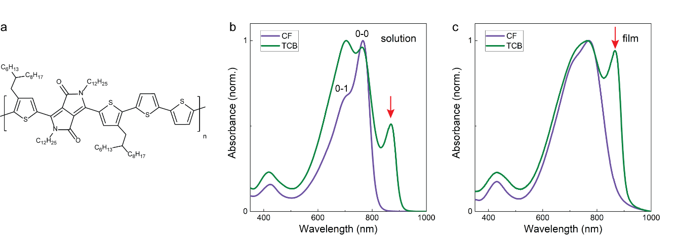
Polymorphism is the ability of a compound to adopt multiple solid state packing motifs and is often found in nature. Polymorphism can have important effects on the physical properties such as optical absorption, emission and electrical conductivity of materials, but of course also provides an excellent platform for investigating structure-property relations. For conjugated polymers it is, however, challenging to efficiently tune the polymorphism in aggregated or semi-crystalline phases due to their conformational freedom and anisotropic nature. We generated two distinct aggregated, semi-crystalline phases based on a low-bandgap diketopyrrolopyrrole polymer (Figure 1a) through tuning solvent quality.

Figure 1. a, Chemical structure of the polymer used in this study. b,c, UV-vis-NIR absorption spectra of polymer (b) solutions and (c) films with chloroform (CF) or 1,2,4-trichlorobenzene (TCB) as solvents. The red arrows indicate the extra absorption peak induced by TCB, suggesting the formation of the second aggregated polymorph (β2).
When the polymer is dissolved in chloroform (CF), the resultant solution exhibits a typical absorption spectrum with an intense first (0-0) vibronic band and a less intense (0-1) vibronic progression at shorter wavelengths, indicative of the first aggregated phase (β1), as shown in Figure 1b. Surprisingly, the solvent of 1,2,4-trichlorobenzene (TCB) results in a completely new absorption peak at 870 nm (indicated by the red arrow), suggesting the generation of the second aggregated polymorph (β2) with higher molecular order. Such rarely reported second (β2) polymorph shows not only a lower optical band gap but also an enhanced photoluminescence. More importantly, these two distinctly different polymorphs are also retained in thin films (Figure 1c), with closer polymer packing for β2 determined from X-ray measurement.

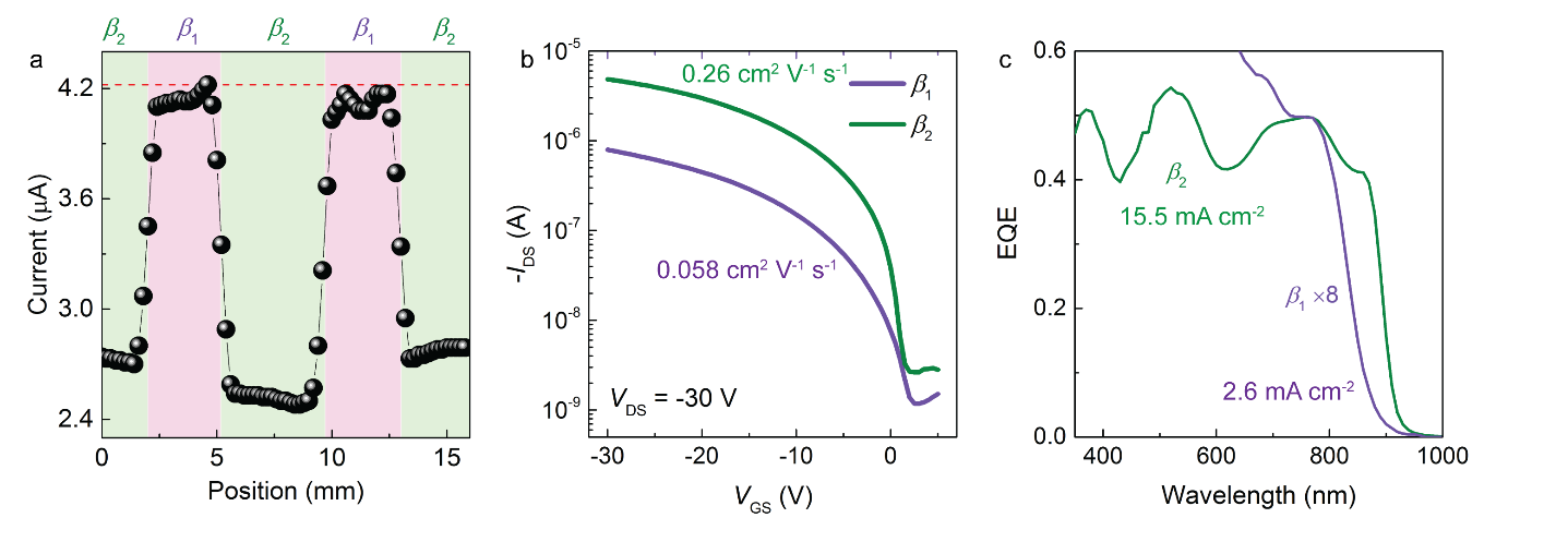
Figure 2. a, Location-dependent functionality by measuring transmitted light at 860 nm as a function of patterned polymorph position. b, Performance of polymer field-effect transistors fabricated by different polymorphs. c, External quantum efficiency (EQE) with AM1.5G solar spectrum of polymer:[70]PCBM solar cells by different polymorphs.
Due to the low band gap of β2 polymorph, the location-dependent functionality can be realized by recording the transmitted light at 860 nm after patterning two polymorphs for thin films (Figure 2a). On the other hand, the polymorphism is found to critically affect the performance of electronic devices. Compared to β1, the closer polymer packing of β2 efficiently promotes the charge transport in field-effect transistors, resulting in 4-fold higher mobility (Figure 2b). In addition, the β2 polymorph remarkably boosts the device performance of solar cells made by polymer:[70]PCBM blends, with the increase of power conversion efficiency from 1.2% to 6.4%, from two aspects (Figure 2c). First, the β2 polymorph forms fibrillar microstructure in the photoactive layer, facilitating exciton diffusion and charge separation. Second, the additional absorption peak of β2 absorbs more light than β1, contributing to the noticeable external quantum efficiency (EQE) at longer wavelength. As a result, the short-circuit current density that is integrated from EQE is significantly enhanced from 2.6 to 15.5 mA cm-2.
This study proposes a simple approach for tuning the polymorphism of conjugated polymers in both solution and solid state, and the characterization provides insights into the structure-property relation of next-generation devices for plastic electronics.
Mengmeng Li and René Janssen
For more details, please see: https://www.nature.com/articles/s41467-019-10519-z
Follow the Topic
-
Nature Communications
An open access, multidisciplinary journal dedicated to publishing high-quality research in all areas of the biological, health, physical, chemical and Earth sciences.
Related Collections
With Collections, you can get published faster and increase your visibility.
Women's Health
Publishing Model: Hybrid
Deadline: Ongoing
Biosensing
Publishing Model: Hybrid
Deadline: Jun 30, 2026


Please sign in or register for FREE
If you are a registered user on Research Communities by Springer Nature, please sign in