Remote epitaxy towards high-quality freestanding semiconductors
Published in Electrical & Electronic Engineering

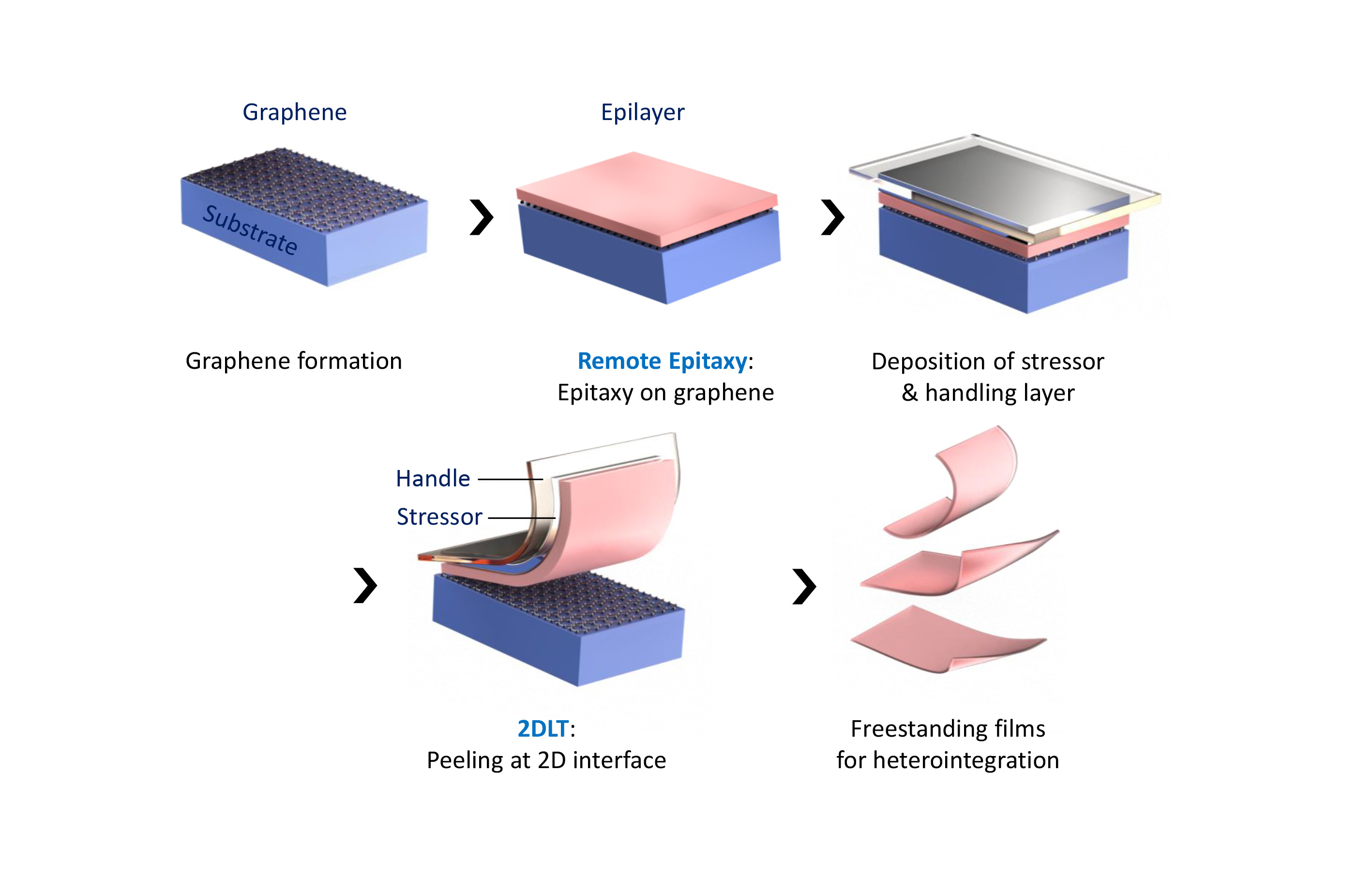
Remote epitaxy is an emergent novel technology that can grow and exfoliate free-standing single-crystalline thin films and structures from the 2D van der Waals materials interface [1, 2]. 2D material-assisted layer transfer technique (2DLT) [3] is the corresponding technique to delaminate and transfer the freestanding semiconductors membranes out of the host substrate to other arbitrary target substrates of interest. This method can not only enable diverse new hetero-integration choices for diverse functional high-quality materials thin films [4, 5], but also enable potentially flexible and stretchable electronic and optoelectronics applications as well [6].

Despite that the principle of remote epitaxy looks simple, it could be challenging to implement due to the stringent requirements for 2D-materials-coated substrate preparation and procedure control. In a recent review paper published on Nature Reviews Methods Primers (article info detailed as below), extensive guidelines on remote epitaxy techniques are elaborated, from preparing 2D materials to epitaxy processes and layer transfer methods. Key considerations and characterization techniques are provided for respective families of materials, as long as their applications for different devices and engineering systems.
Article info:
Hyunseok Kim, Celesta S. Chang, Sangho Lee, et al, Remote epitaxy, Nature Reviews Methods Primers, 2, 40 (2022).
Link: https://www.nature.com/articles/s43586-022-00122-w
Primer view: https://www.nature.com/articles/s43586-022-00134-6
DOI: 10.1038/s43586-022-00122-w
References:
[1] Remote epitaxy through graphene for two-dimensional material based layer transfer, Nature, 544, 340–343 (2017).
[2] Remote epitaxy, Nature Reviews Methods Primers, 2, 40 (2022).
[3] Controlled crack propagation for atomic precision handling of wafer-scale two-dimensional materials, Science, 362, 665-670 (2018).
[4] Heterogeneous integration of single-crystalline complex-oxide membranes, Nature, 578, 75-81 (2020).
[5] Integration of bulk materials with two-dimensional materials for physical coupling and applications, Nature Materials, 18, 550–560 (2019).
[6] Multifunctional materials for implantable and wearable photonic healthcare devices, Nature Reviews Materials, 5, 149–165 (2020).


Please sign in or register for FREE
If you are a registered user on Research Communities by Springer Nature, please sign in