Wafer-scale single-domain 2D materials enabled by geometric confinement
Published in Electrical & Electronic Engineering
Two-dimensional (2D) materials and their heterostructures have ushered massive novel electronic and optoelectronic applications [1-3]. However, despite the enormous endeavors made on 2D materials with massive record-setting devices reported in lab, the commercialization path of 2D optical materials-based applications is still largely lagging behind market expectations [4].
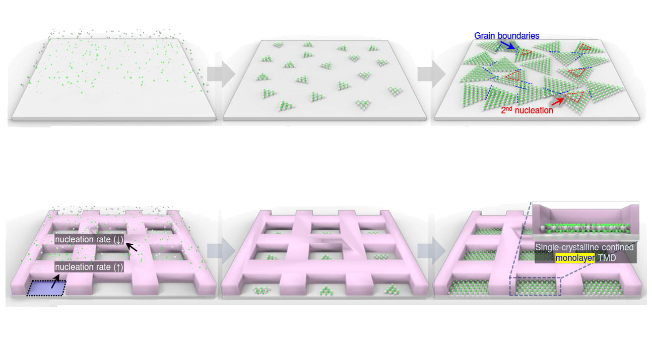
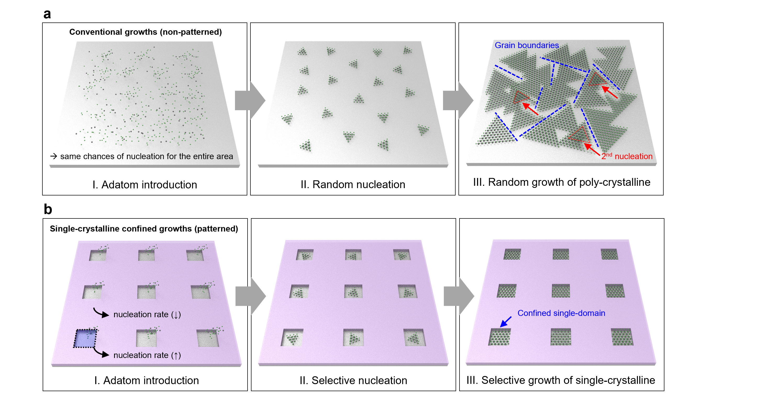
One paramount challenge is the trade-off between material quality and the cost of mass-production throughput. Mechanical exfoliations-based approaches, for example, can provide 2D flakes with high quality, but it generally remains extremely laborious with low yield. Growth-based methods such as chemical vapor depositions (CVDs) can massively produce 2D materials with high scalability. Nevertheless, these strategies are typically plagued by grain boundaries and ununiformed nucleation (e.g. a hybrid of 0~2 monolayers) over large wafer-scale (Fig. 1a). Three critical challenges thus emerged: (1) the precise kinetic control of layer by-layer 2D material growth, (2) Maintaining single-domain during the growth, and (3) wafer-scale controllability of monolayer numbers and crystallinity.
As most electronic and photonic applications only use a relatively small area of 2D materials at desired locations, if we can achieve location-selective 2D material growth with single-crystallinity, (mono)layer controllability, and large area over wafer-scale, it could be potentially hatched as a game-changer for 2D electronics and optoelectronics society by offering a transfer-free paradigm with comparable 2D material quality to mechanical exfoliations for diverse applications.
Recently, a group of researchers from Massachusetts Institute of Technology and other international universities has proposed a new 2D transition metal dichalcogenides (TMDs) monolayers (ML) and heterostructures synthesis strategy to simultaneously tackle the abovementioned three issues. By using patterned oxide mask on sapphire and (ALD-grown) HfO2-covered substrates, deterministic confined growth technique is introduced to obtain wafer-scale single-domain 2D monolayer and their heterostructures on potentially arbitrary substrates.
The researchers confine the growth of the first set of nuclei by defining a selective growth area (pocket) via patterning SiO2 masks on 2-inch substrates. Owing to substantial reduction of the growth duration at the few micron-scale SiO2 trenches (Fig. 2), wafer-scale single-domain ML WSe2 arrays are obtained on arbitrary substrates by filling the trenches with a short growth of the first set of nuclei before the 2nd set of nuclei is introduced (thus not requiring epitaxial seedings) (Fig. 1b). Further growth of TMDs with the same principle can lead to the formation of single-domain MoS2/WSe2 heterostructures.

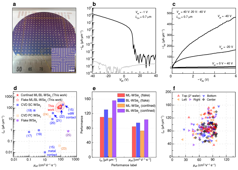
The experimental characterization results of the grown 2D materials are summarized as Fig. 3, where more information can be found in the original article recently published on Nature. The confined geometry allows precise control of the number of monolayers, where the next TMD MLs can be subsequently grown to fill up the trenches of the oxide mask. The field effect transistors (FETs) fabricated on the arrays of single-domain WSe2 over the entire 2-inch wafer show excellent performances approaching to that of mechanically exfoliated WSe2 flakes, with for instance, effective mobility up to 72.8 cm2V–1s–1 for ML-WSe2 and 103.5 cm2V–1s–1 for BL-WSe2.
Article link:
https://www.nature.com/articles/s41586-022-05524-0
Article info:
Ki Seok Kim, Doyoon Lee, Celesta S. Chang, et al. Non-epitaxial single-crystal 2D material growth by geometrical confinement. Nature, 2023.
References:
[1] S.-H. Bae, et al. Science, 362 , 665-670 (2018).
[2] Y. Meng, et al. Nature Reviews Materials 8, 498-517 (2023).
[3] J.-H. Kang, et al. Nature Materials (2023). DOI: 10.1038/s41563-023-01704-z
[4] W. Kong, et al. Nature Nanotechnology 14, 927-938 (2019).
Follow the Topic
-
Nature
A weekly international journal publishing the finest peer-reviewed research in all fields of science and technology on the basis of its originality, importance, interdisciplinary interest, timeliness, accessibility, elegance and surprising conclusions.



Please sign in or register for FREE
If you are a registered user on Research Communities by Springer Nature, please sign in